Method for forming through silicon vias (TSV)

A technology of TSV and deep via, which is applied in the manufacturing of electrical components, circuits, semiconductor/solid-state devices, etc., can solve the problem of limited high frequency performance of TSV, and it is difficult to ensure the side of TSV at the same time. Wall isolation performance and electrical conduction performance and other issues, to achieve the effect of improving reliability and electrical performance

Inactive Publication Date: 2011-10-05
INST OF MICROELECTRONICS CHINESE ACAD OF SCI
View PDF2 Cites 17 Cited by
  • Summary
  • Abstract
  • Description
  • Claims
  • Application Information

AI Technical Summary

Problems solved by technology

[0008] In order to solve the problem that the TSV formation method in the prior art is difficult to ensure the sidewall isolation performance and electrical conduction performance of the TSV at the same time; the sidewall insulating layer is thin, and the high-frequency performance of the TSV is limited. Problem,

Method used


Image

  • Method for forming through silicon vias (TSV)
  • Method for forming through silicon vias (TSV)
  • Method for forming through silicon vias (TSV)

Examples


Embodiment

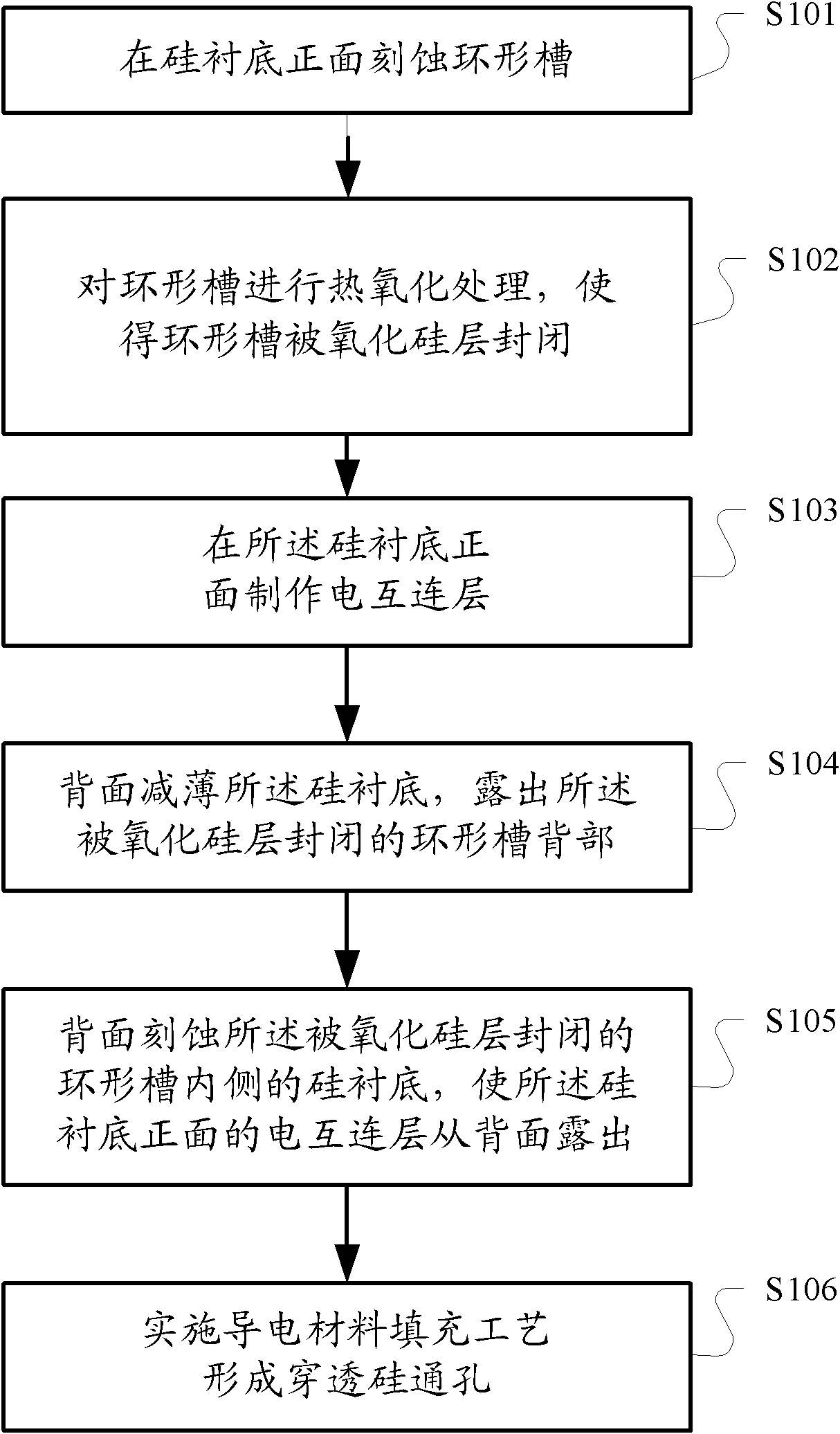
[0039] like figure 1 As shown, the method for forming TSVs provided by the present invention comprises the following steps:

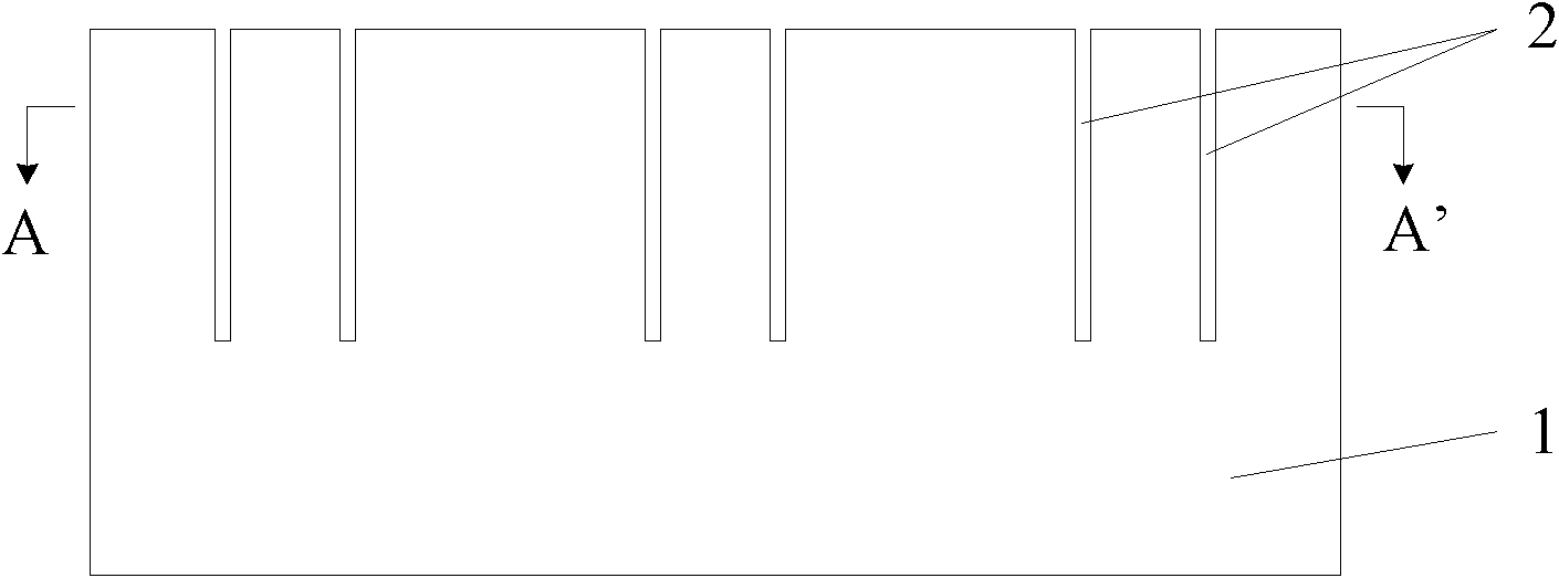
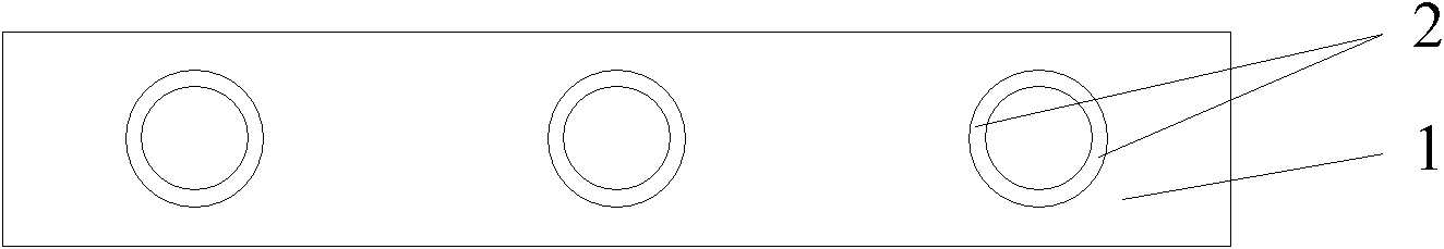
[0040] first step, such as figure 2 and image 3 As shown, an annular groove 2 is etched on the front surface of a silicon substrate 1 .

[0041] The width of the annular groove 2 can range from 0.5 μm to 3 μm, and the depth of the annular groove 2 is equal to or greater than the length of the TSV to be obtained, so as to ensure the processing feasibility and the smooth progress of subsequent steps; the annular groove 2 is in the The width at the opening is equal to or greater than the width of the annular groove 2 at its depth, wherein the difference between the width of the annular groove 2 at the opening and the width of the annular groove 2 at its depth is in the range of 0 to 2 μm to facilitate subsequent processing The silicon oxide layer 3 closes the annular groove 2 . In this embodiment, the method used to etch the annular groove 2 is a dee...


PUM

PropertyMeasurementUnit
Width rangeaaaaaaaaaa

Abstract

The invention discloses a method for forming through silicon vias (TSV), belonging to the semiconductor device manufacture, microelectronic packaging and three dimensional integration field. The method comprises the following steps: (1) etching annular grooves on the right side of a silicon substrate; (2) carrying out a thermal oxidation treatment on the annular grooves; (3) making an electrical interconnection layer on the right side of the silicon substrate; (4) thinning the silicon substrate from the back side of the silicon substrate; (5) etching the silicon substrate in the annular grooves which are sealed by an oxygen ambient silica layer to remove the oxygen ambient silica layer totally and forming deep holes in the inner side of the annular grooves; and filling conductive material in the deep holes to form the through silicon vias (TSV). By using the method provided in the invention, the through silicon vias (TSV) using high quality thick oxygen ambient silica layer, metallic sidewall isolation and conductive filling material can be obtained, and the reliability and electricity performance of the through silicon vias (TSV) are improved.

Description

technical field [0001] The invention relates to the technical fields of semiconductor manufacturing, microelectronic packaging and three-dimensional integration, in particular to a method for forming through-silicon holes. Background technique [0002] Through-Silicon-Via (TSV) is an electrical connection through the chip, which can conduct signals from one side of the chip to the other side of the chip, and realize the three-dimensional structure of multi-layer chips by combining chip stacking technology. integrated. Compared with the traditional wire bonding technology, the use of TSVs can effectively shorten the length of interconnection lines between chips, thereby improving the signal transmission performance and operating frequency of electronic systems, which is an important direction for the development of semiconductor technology in the future. How to The formation of through-silicon vias is the core to realize the three-dimensional integration of multi-layer chips...

Claims


Application Information

Patent Timeline
IPC IPC(8): H01L21/768H01L21/60
Inventor 宋崇申
Owner INST OF MICROELECTRONICS CHINESE ACAD OF SCI
Why Eureka
Try Eureka