
Three-dimensional packaging method

A three-dimensional packaging and substrate technology, applied in semiconductor devices, electrical components, circuits, etc., to achieve the effect of low injection cost and easy integration

Inactive Publication Date: 2011-10-12
SHANGHAI SIMGUI TECH
View PDF4 Cites 2 Cited by
  • Summary
  • Abstract
  • Description
  • Claims
  • Application Information

AI Technical Summary

Problems solved by technology

However, this method needs to form a peeling layer by means of ion implantation in the substrate where the device has been formed. The ion implantation will inevitably affect the formed device layer, and this process cannot avoid the use of expensive SOI substrates.

Method used


Image

  • Three-dimensional packaging method
  • Three-dimensional packaging method
  • Three-dimensional packaging method

Examples


Embodiment Construction

[0012] Next, a specific implementation manner of a three-dimensional packaging method of the present invention will be described in detail with reference to the accompanying drawings.

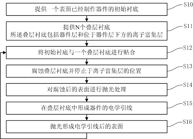
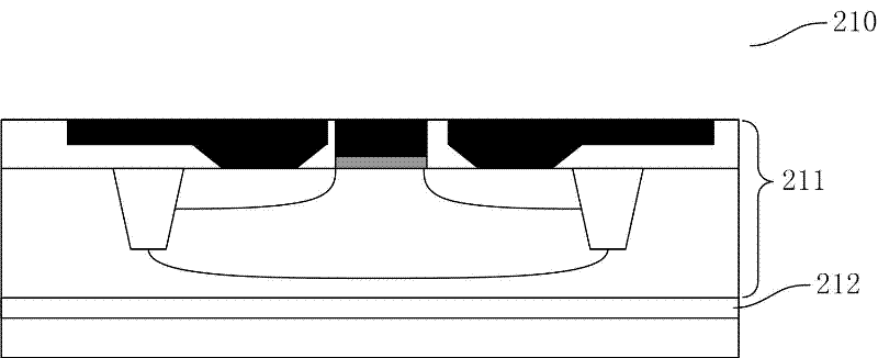
[0013] attached figure 1 Shown is a schematic diagram of the implementation steps of the method described in this specific embodiment, including: step S10, providing an initial substrate whose surface has been fabricated with devices; step S11, providing N stacked substrates, the stacked substrates including devices layer and the ion-enriched layer below the device layer; Step S12, attaching the initial substrate to a stacked substrate; Step S13, corroding the stacked substrate and stopping at the position of the ion-enriched layer; Step S14, Polishing the corroded surface; Step S15, forming electrical leads of the device in the laminated substrate; Step S16, polishing the surface after forming the electrical leads, forming a three-dimensional packaging structure with two device layers. The ab...


PUM


Abstract

The invention relates to a three-dimensional packaging method which comprises the following steps: providing an initial substrate of which a device is made on the surface; providing N laminated substrates, wherein the laminated substrate comprises a device layer and an ion collection layer below the device layer; gluing the initial substrate and a laminated substrate; etching the laminated substrate and stopping at the position of the ion collection layer; forming an electricity lead in the laminated substrate; repeating the steps and bonding the N laminated substrates in sequence to form a three-dimensional packaging structure with N+1 device layers, wherein N is an integer greater than one.

Description

technical field [0001] The invention relates to a method for preparing a silicon-on-insulator material, in particular to a three-dimensional packaging method. Background technique [0002] In order to realize the three-dimensional integration of integrated circuit chips, it is necessary to overlap silicon wafers or chips that have already completed circuits, and a good electrical signal path needs to be ensured between the overlapping chips. The way to achieve this is through silicon via (TSV) technology. The existing technology usually uses bulk silicon wafers, which are directly thinned to a thickness of about 100um after the device is completed. This process is limited by silicon wafer thinning technology and cannot be made into very thin silicon wafers, making it difficult to realize the through-hole process. An improved method is to use an expensive SOI chip, the top layer of silicon is used as the device layer, and the substrate layer is used as the sacrificial layer. ...

Claims


Application Information

Patent Timeline
IPC IPC(8): H01L21/98
CPCH01L2924/13091H01L2224/16145H01L2924/00
Inventor 张峰曹共柏魏星王文宇王曦
Owner SHANGHAI SIMGUI TECH
Learn More