Method for improving antistatic capability of gallium nitride based light emitting diode

A light-emitting diode, gallium nitride-based technology, applied in chemical instruments and methods, circuits, electrical components, etc., can solve the problems of poor quality of epitaxial materials, reduce the density of threading dislocations in epitaxial layers, etc., to improve antistatic ability. , Improve antistatic ability, reduce the effect of electrostatic accumulation damage

Inactive Publication Date: 2011-10-12
INST OF SEMICONDUCTORS - CHINESE ACAD OF SCI
View PDF6 Cites 21 Cited by
  • Summary
  • Abstract
  • Description
  • Claims
  • Application Information

AI Technical Summary

Problems solved by technology

[0008] In view of this, the main purpose of the present invention is to provide a method for improving the antistatic ability of gallium nitride-based light-emitting diodes, by inserting an aluminum gallium nitride / gallium nitride super The lattice insertion layer modulates and releases the stress caused by lattice mismatch in the epitaxial layer, and makes the dislocations in the GaN epitaxial layer divert and merge, reducing the density of threading dislocations in the subsequently grown epitaxial layer and solving the problem of epitaxy. The problem of poor material quality can be achieved to improve the material quality and improve the antistatic ability of light-emitting diodes

Method used


Image

  • Method for improving antistatic capability of gallium nitride based light emitting diode
  • Method for improving antistatic capability of gallium nitride based light emitting diode
  • Method for improving antistatic capability of gallium nitride based light emitting diode

Examples


Embodiment Construction

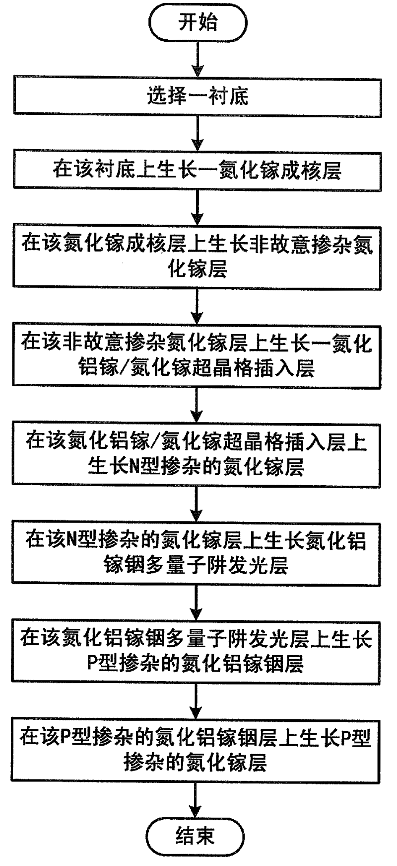
[0035] In order to make the object, technical solution and advantages of the present invention clearer, the present invention will be described in further detail below in conjunction with specific embodiments and with reference to the accompanying drawings.

[0036] The key point of the present invention is to proceed from the epitaxial growth mechanism and the dislocation control of the epitaxial layer, and change the distribution of dislocations in the epitaxial layer by introducing the AlGaN / GaN superlattice to make them divert and merge, thereby reducing the subsequent growth rate. The dislocation density in GaN materials improves the quality of materials and improves the antistatic ability of light-emitting diodes.

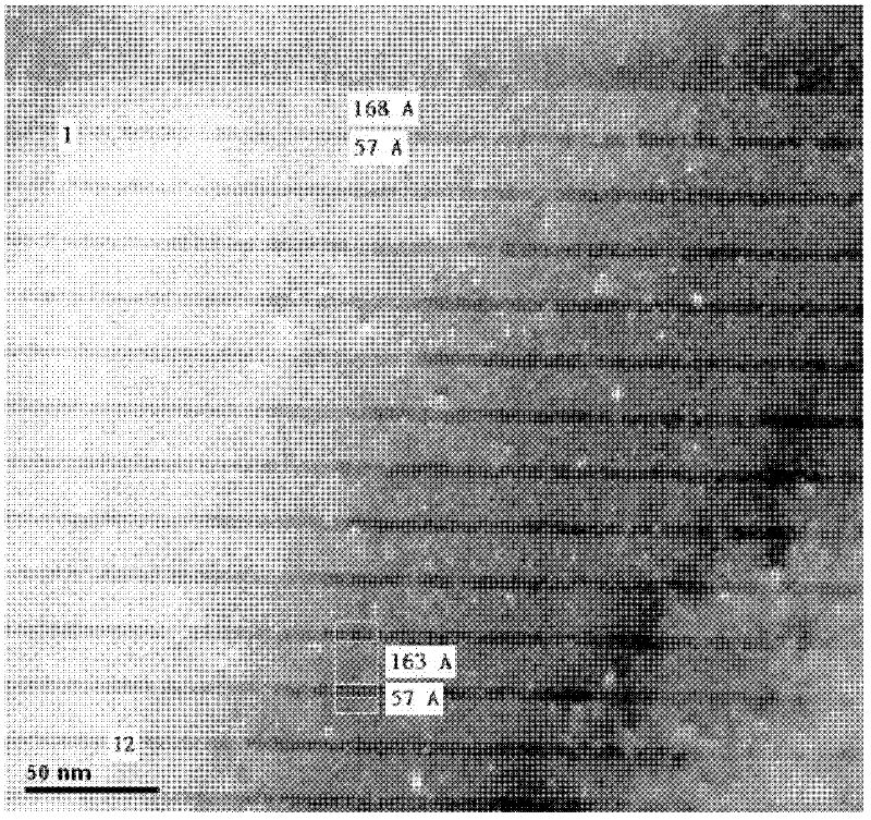
[0037] The method for improving the antistatic ability of gallium nitride-based light-emitting diodes provided by the present invention is to insert an aluminum gallium nitride / gallium nitride superlattice insertion layer between unintentionally doped GaN and ...


PUM

PropertyMeasurementUnit
sizeaaaaaaaaaa
thicknessaaaaaaaaaa
thicknessaaaaaaaaaa

Abstract

The invention discloses a method for improving antistatic capability of a gallium nitride based light emitting diode. The method comprises the following steps: selecting a substrate; growing a gallium nitride nucleating layer on the substrate; growing an involuntary doped gallium nitride layer on the gallium nitride nucleating layer; growing an aluminum gallium nitride/ gallium nitride superlattice insertion layer on the involuntary doped gallium nitride layer; growing an N-type doped gallium nitride layer on the aluminum gallium nitride/ gallium nitride superlattice insertion layer; growing an indium gallium aluminum nitride multiple quantum-well light-emitting layer on the N-type doped gallium nitride layer; growing a P-type doped indium gallium aluminum nitride layer on the indium gallium aluminum nitride multiple quantum-well light-emitting layer; and growing a P-type doped gallium nitride layer on the P-type doped indium gallium aluminum nitride layer. By utilizing the method provided by the invention, the stress caused by lattice mismatch in an epitaxial layer can be modulated, simultaneously the dislocation in the epitaxial layer of the GaN (gallium nitride) can be deflected and combined, thus the density of threading dislocation in the epitaxial layer developed subsequently is reduced, the material quality is improved, and the antistatic capability of the light emitting diode is improved.

Description

technical field [0001] The invention belongs to the technical field of preparation of gallium nitride-based light-emitting diodes, in particular to a method for improving the antistatic ability of gallium nitride-based light-emitting diodes. Background technique [0002] The current semiconductor lighting technology based on GaN-based light-emitting diodes (LEDs) is penetrating into all aspects of social life, such as landscape lighting, special lighting, and liquid crystal backlight lighting. However, due to the inherent defects, high dislocation density, and poor material quality of III-nitrides, semiconductor lighting devices based on III-nitrides have poor antistatic capabilities, which limits their further entry into the high-end application market. In order for semiconductor lighting to enter general lighting, in addition to the continuous improvement of efficiency, the improvement of antistatic ability is also a very urgent demand. [0003] At present, many solutions...

Claims


Application Information

Patent Timeline
Patent Type & Authority Applications(China)
IPC IPC(8): H01L33/00H01L33/06C30B29/68C30B29/40C30B29/38
Inventor 李志聪姚然王兵梁萌李鸿渐李盼盼李璟王国宏李晋闽
Owner INST OF SEMICONDUCTORS - CHINESE ACAD OF SCI
Why Eureka
Try Eureka