Precise measuring method of crystalline silicon body lifetime

A technology for accurate measurement and bulk life, applied in semiconductor working life testing, single semiconductor device testing, semiconductor characterization, etc., can solve problems such as trouble

CN106680687AInactive Publication Date: 2017-05-17ZHEJIANG NORMAL UNIVERSITY
4 Cites 9 Cited by

Patent Information

Authority / Receiving Office
CN · China
Current Assignee / Owner
Publication Date
2017-05-17
Estimated Expiration
Not applicable · inactive patent

Smart Images

  • Figure 1
    Figure 1
  • Figure 2
    Figure 2
  • Figure 3
    Figure 3
Patent Text Reader

Abstract

The invention discloses a precise measuring method of crystalline silicon body lifetime. The precise measuring method of the crystalline silicon body lifetime comprise the steps that minority carrier lifetime is measured through a quasi-steady-state photoelectric conduction method, a true value of the silicon wafer minority carrier lifetime can be obtained accurately and quickly through a quasi-steady-state minority carrier lifetime measuring method, the effective minority carrier lifetime comprises a body lifetime and a surface recombination lifetime, on the precise of the same silicon wafer recombination conditions, the true body lifetime of the silicon wafer is obtained by calculating through formulas, and the calculated true body lifetime of the silicon wafer is similar to the body lifetime measured through the photoconductive decay method. The method for measuring the minority carrier lifetime through the quasi-steady-state photoelectric conduction method and obtaining the true body lifetime through calculation has the advantages of being simple, fast, free of contamination and the like.
Need to check novelty before this filing date? Find Prior Art

Description

technical field

[0001] The invention belongs to the technical field of photovoltaic cells, and in particular relates to a method for accurately measuring the lifetime of a crystalline silicon body. Background technique

[0002] The lifetime of minority carriers in semiconductors plays a decisive role in the current gain, forward voltage drop and switching speed of bipolar devices. The conversion efficiency of semiconductor solar cells, the detection rate of semiconductor detectors and the luminous efficiency of light-emitting diodes are also related to the lifetime of carriers. Therefore, the measurement of the minority carrier lifetime in semiconductors has been widely valued.

[0003] When measuring the minority carrier lifetime, in addition to the recombination centers generated by heavy metal impurities in the silicon wafer, single crystal surface defects will also play the role of recombination centers, so the measured value of the non-equilibrium minority carrier life...

Examples

Embodiment Construction

[0028] The specific implementation is as follows:

[0029] In the first step, two pieces of B-doped p-type single crystal Si obtained from the same part of the sample silicon ingot are taken, and the thicknesses are 300 μm and 500 μm respectively.

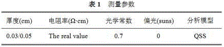
[0030] In the second step, the specified minority carrier concentration is 4´10 measured by the quasi-steady-state photoconductivity method 14 cm -3 When the effective minority carrier lifetime is obtained, the effective minority carrier lifetime before cleaning is obtained. The following table shows the parameters set when using the quasi-steady-state photoconductivity method for measurement.

[0031]

[0032] The specific measurement method is as follows:

[0033] 1) A long-wavelength and slowly decaying pulse light is provided by a xenon flash lamp; the decay constant of the pulse light in a steady state is at least ten times slower than the minority carrier lifetime, and the decay constant of the flash lamp is about 2ms wh...