Large-mismatch silicon-based substrate antimonide transistor with high electron mobility and manufacturing method thereof

A high electron mobility, antimonide technology, used in semiconductor/solid-state device manufacturing, circuits, electrical components, etc., can solve problems such as lattice mismatch

Active Publication Date: 2012-01-18
INST OF SEMICONDUCTORS - CHINESE ACAD OF SCI
View PDF3 Cites 12 Cited by
  • Summary
  • Abstract
  • Description
  • Claims
  • Application Information

AI Technical Summary

Problems solved by technology

However, the serious mismatch of the crystal lattice is also t

Method used


Image

  • Large-mismatch silicon-based substrate antimonide transistor with high electron mobility and manufacturing method thereof
  • Large-mismatch silicon-based substrate antimonide transistor with high electron mobility and manufacturing method thereof
  • Large-mismatch silicon-based substrate antimonide transistor with high electron mobility and manufacturing method thereof

Examples


Embodiment Construction

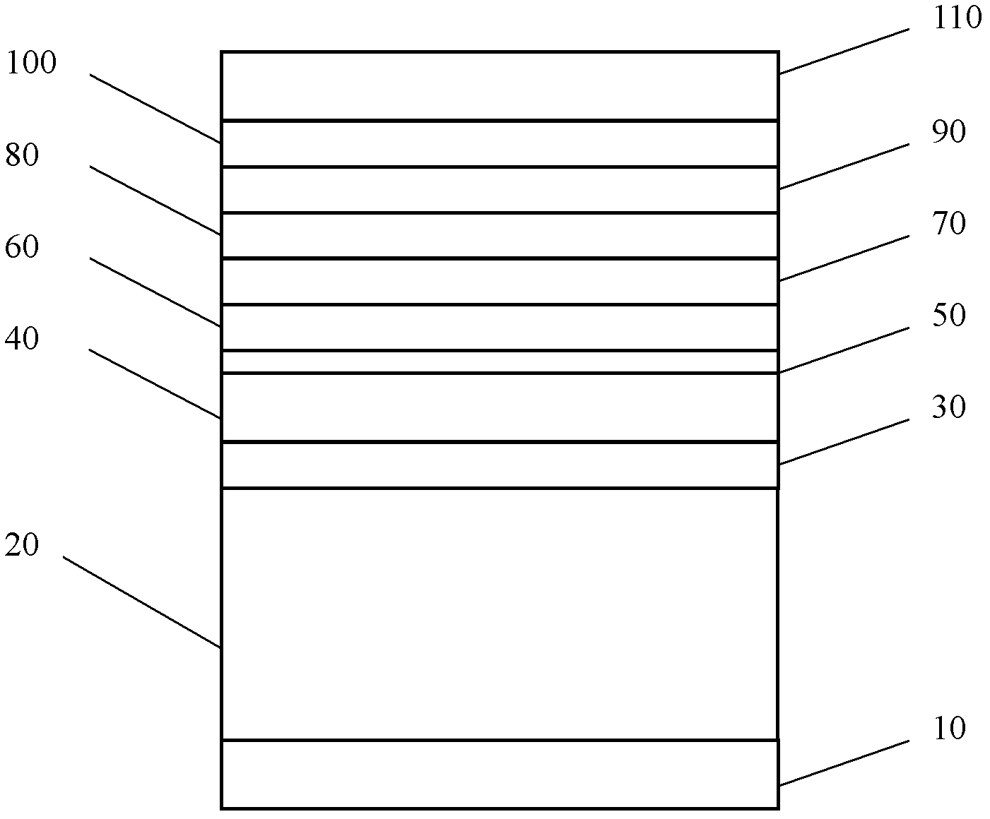
[0023] see figure 1 , figure 2 and image 3 As shown, the present invention provides a large mismatch silicon-based substrate antimonide high electron mobility transistor, including:

[0024] A substrate 10, the material of the substrate 10 is Si; Si material is one of the most widely used semiconductor materials, Si technology is quite mature in semiconductor technology, and technologies such as surface treatment of Si substrates are becoming more and more perfect, so The selection of Si substrate can greatly reduce the workload. At the same time, the selection of Si substrate facilitates the integration of the antimonide high electron mobility transistor with other silicon-based devices in the future, so that devices with different functions can be obtained;

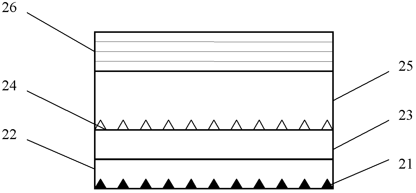
[0025] A composite buffer layer 20, grown on the substrate 10, the composite buffer layer 20 includes:

[0026] An AlSb quantum dot structure 21, the height and diameter of the AlSb quantum dot are respectively a...


PUM

PropertyMeasurementUnit
Thicknessaaaaaaaaaa
Thicknessaaaaaaaaaa

Abstract

The invention provides a large-mismatch silicon-based substrate antimonide transistor with high electron mobility. The large-mismatch silicon-based substrate antimonide transistor comprises a substrate, a composite buffering layer growing on the substrate, an insert layer growing on the composite buffering layer, an AlSb isolation layer growing on the insert layer, a sub channel layer growing on the AlSb isolation layer, an antimonide lower potential barrier layer growing on the sub channel layer, an InAs channel layer growing on the antimonide lower potential barrier layer, an antimonide isolation layer growing on the InAs channel layer, a doping layer growing on the antimonide isolation layer, wherein the doping layer is InAs doped with a Si plane or delta doping of Te; an upper potential barrier layer growing on the doping layer, wherein the upper potential barrier layer is a composite potential barrier layer consisting of an AlSb layer and an InAlAs layer; and an InAs cap layer growing on the upper potential barrier layer, wherein the InAs cap layer is an unintentionally doped InAs or n type doped InAs.

Description

technical field [0001] The invention belongs to the technical field of semiconductors, in particular to high electron mobility transistors based on large mismatch silicon-based substrate antimonides and a manufacturing method. technical background [0002] Antimonide semiconductors refer to binary or multi-component III-V compound semiconductor materials containing antimony elements. Since the lattice constant is close to The binary antimonide semiconductor materials AlSb, GaSb, InSb and InAs are often referred to as Material systems, they cover a large bandgap range, and have excellent properties such as high electron mobility and high electron saturation velocity. These characteristics create a broad space for the manufacture of high-speed, low-power microelectric and optoelectronic devices. In high-speed compound semiconductors, antimonide high electron mobility transistors play a pivotal role. High electron mobility transistors based on III-V compound semiconductors ...

Claims


Application Information

Patent Timeline
IPC IPC(8): H01L29/778H01L21/335
Inventor 张雨溦张杨曾一平
Owner INST OF SEMICONDUCTORS - CHINESE ACAD OF SCI
Why Eureka
Try Eureka