Ultraviolet light-emitting device with a heavily doped strain-management interlayer

a strain-management interlayer and ultra-violet light technology, which is applied in the direction of basic electric elements, semiconductor devices, electrical equipment, etc., can solve the problems of high forward voltage for uv leds, deterioration of the p-contact layer surface morphology and conductivity, and dislocation generation and growth surface roughening of the n-algan layer, etc., to achieve efficient and cost-effective approach, improve material quality and device performance

Active Publication Date: 2017-06-13
BOLB
View PDF6 Cites 10 Cited by
  • Summary
  • Abstract
  • Description
  • Claims
  • Application Information

AI Technical Summary

Benefits of technology

[0006]The present invention discloses an efficient and cost-effective approach for strain, especially compressive strain management, and LED, especially UV LED structures with such strain management of greatly improved material quality and device performance.

Problems solved by technology

Compressive strain of this size can lead to dislocation generation and growth surface roughening of the n-AlGaN layer.
Coherent AlGaN / AlGaN MQW is essential for high efficient UV emission, however, the thus fully strained MQW because of the AlGaN piezoelectric effect can lead to high forward voltage for the UV LEDs.
The large compressive strain here can deteriorate p-contact layer surface morphology and conductivity.
These constraints make superlattice approach for strain management impractical or inconvenient for some interfaces within a UV light emitter structure.

Method used


Image

  • Ultraviolet light-emitting device with a heavily doped strain-management interlayer
  • Ultraviolet light-emitting device with a heavily doped strain-management interlayer
  • Ultraviolet light-emitting device with a heavily doped strain-management interlayer

Examples


Embodiment Construction

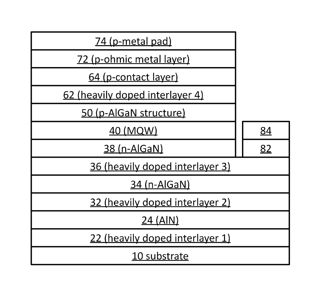
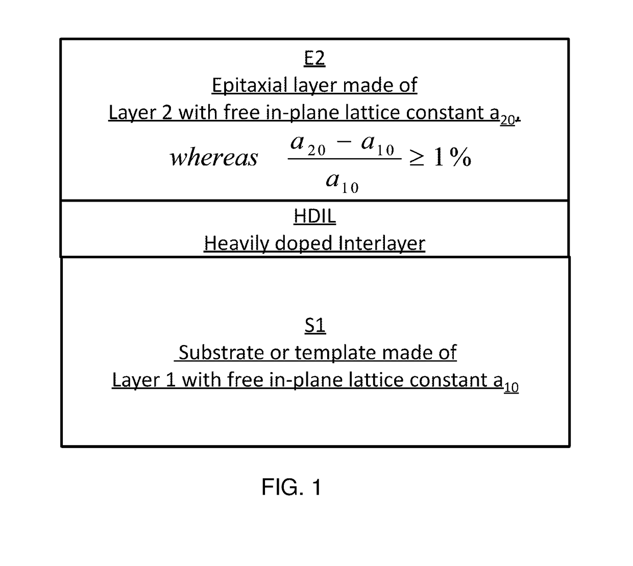
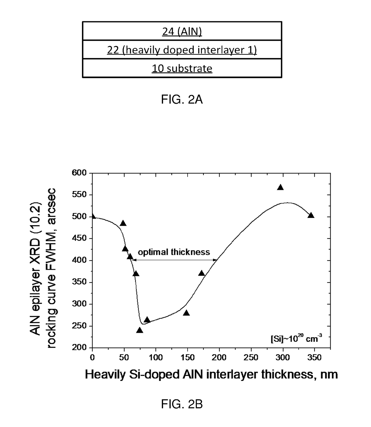
[0038]The present invention discloses a strain management approach and LED, especially UV LED devices incorporated with compressive strain management with improved quantum efficiencies. Throughout the specification, the term III-nitride or nitride in general refers to metal nitride with cations selecting from group IIIA of the periodic table of the elements. That is to say, III-nitride includes AlN, GaN, InN and their ternary (AlGaN, InGaN, InAlN) and quaternary (AlInGaN) alloys. In this specification, a quaternary can be reduced to a ternary for simplicity if one of the group III elements is significantly small. For example, if the In-composition in a quaternary AlInGaN is significantly small, smaller than 1%, then this AlInGaN quaternary can be shown as ternary AlGaN for simplicity. Using the same logic, a ternary can be reduced to a binary for simplicity if one of the group III elements is significantly small. For example, if the In-composition in a ternary InGaN is significantly...


PUM


Abstract

A heteroepitaxy strain-management structure for a light emitting device includes: a substrate or template; an epitaxial layer to be epitaxially formed over the substrate or template, wherein a calculated in-plane compressive strain to be exerted by the substrate or template to the epitaxial layer is equal to or larger than 1%; and a heavily doped interlayer inserted in-between the epitaxial layer and the substrate or template; wherein the heavily doped interlayer is of substantially the same material composition as that of the epitaxial layer, with a thickness of 40-400 nm, and doped at a doping level in the range of 5×10¹⁹ to 5×1020 cm−3. Also provided is an ultraviolet light emitting device having a heteroepitaxy strain-management structure.

Description

1. FIELD OF THE INVENTION[0001]The present invention relates in general to semiconductor epitaxial layer structure having two adjacent layers with in-plane compressive strain and a heavily doped strain-management interlayer inserted therebetween, and to a group III nitride ultraviolet light emitting device having a heavily doped strain-management interlayer.2. DESCRIPTION OF THE RELATED ART[0002]Nitride compound semiconductors such as InN, GaN, AlN, and their ternary and quaternary alloys are viewed as very important optoelectronic materials. Depending on alloy composition, nitride compounds can enable ultraviolet (UV) emissions ranging from 410 nm down to approximately 210 nm. This includes UVA (400-315 nm), UVB (315-280 nm), and part of UVC (280-210 nm) regimes. UVA emissions are leading to revolutions in curing industry, and UVB and UVC emissions owing to their germicidal effect are looking forward to general adoption in food, water, air, and surface disinfection businesses. Comp...

Claims


Application Information

Patent Timeline
Patent Type & Authority Patents(United States)
IPC IPC(8): H01L33/12H01L33/06H01L33/32H01L33/00
CPCH01L33/12H01L33/0025H01L33/32H01L33/06
Inventor ZHANG, JIANPINGZHOU, LING
Owner BOLB
Why Eureka
Try Eureka