Method and system for realizing high-resolution analog-to-digital conversion by low-resolution ADC (Analog to Digital Converter)
An analog-to-digital conversion, high-resolution technology, applied in the electrical field, can solve problems such as data transmission link delay, and achieve the effect of increasing data transmission rate, reducing delay, and being less susceptible to noise and interference.
- Summary
- Abstract
- Description
- Claims
- Application Information
AI Technical Summary
Problems solved by technology
Method used
Image

Examples
Embodiment Construction
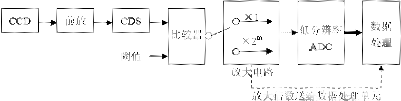
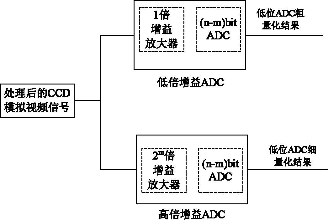
[0048] The invention provides a method for realizing high-resolution analog-to-digital conversion by a low-resolution ADC, the method comprising the following steps:
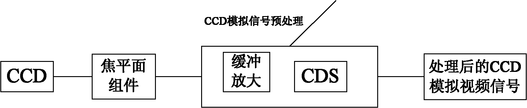
[0049] 1) Post-stage preprocessing of the CCD analog signal generated by the FPA (focal plane assembly):
[0050] The purpose of post-stage preprocessing of the CCD analog signal generated by the FPA (focal plane assembly) is to make the output signal have the same change trend as the illuminance received by the CCD sensor, and to suppress the interference introduced during the transmission process and minimize the noise in the CCD output signal. Reset noise (kTC noise). Usually available figure 2 In order to suppress the interference introduced in the transmission process, the buffer circuit first buffers the received video signal, which is realized by an operational amplifier, and the gain is -1 times. The purpose of the correlated double sampling circuit CDS is to reduce the reset noise (kTC noise) of the ...
PUM
 Abstract
Description
Claims
Application Information
 - R&D
- Intellectual Property
- Life Sciences
- Materials
- Tech Scout
- Unparalleled Data Quality
- Higher Quality Content
- 60% Fewer Hallucinations
Browse by: Latest US Patents, China's latest patents, Technical Efficacy Thesaurus, Application Domain, Technology Topic, Popular Technical Reports.
© 2025 PatSnap. All rights reserved.Legal|Privacy policy|Modern Slavery Act Transparency Statement|Sitemap|About US| Contact US: help@patsnap.com