Visible photoelectrochemical detector based on one-dimensional silicon nanostructure array

A technology of silicon nano-array and photoelectrochemistry, which is applied in the direction of photometry, optics, and optical components using electric radiation detectors, and can solve the problems of multiple and complex equipment

Active Publication Date: 2011-10-26
BEIJING NORMAL UNIVERSITY
View PDF2 Cites 15 Cited by
  • Summary
  • Abstract
  • Description
  • Claims
  • Application Information

AI Technical Summary

Problems solved by technology

The performance research of a single one-dimensional silicon nanostructure generally needs to be integrated into a micro-nano prototype device, and the change of its corresponding physic

Method used


Image

  • Visible photoelectrochemical detector based on one-dimensional silicon nanostructure array
  • Visible photoelectrochemical detector based on one-dimensional silicon nanostructure array
  • Visible photoelectrochemical detector based on one-dimensional silicon nanostructure array

Examples


specific Embodiment approach 1

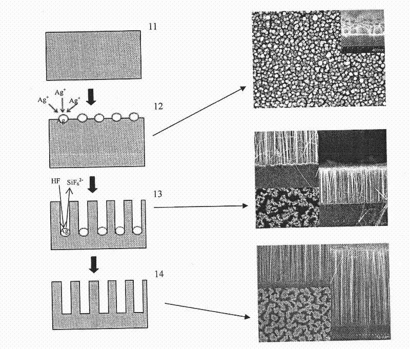
[0046] 1. Fabrication of n-type one-dimensional silicon nanostructure arrays by metal-catalyzed chemical etching

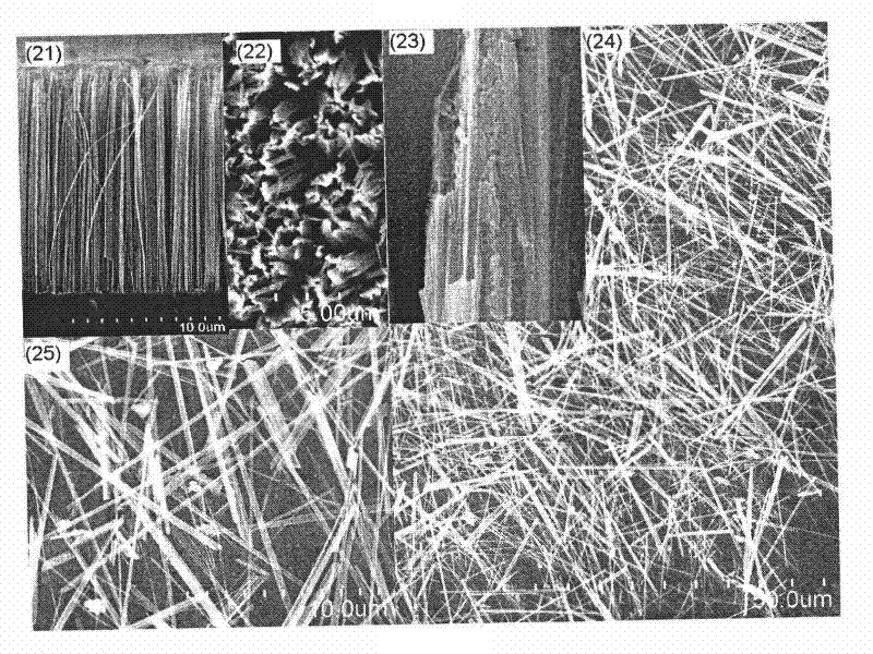
[0047] figure 1 It is a schematic diagram of the process of preparing a one-dimensional silicon nanostructure array by metal-catalyzed chemical etching on a (100) single crystal silicon substrate and a typical scanning electron microscope image of the corresponding stage. The preparation process is divided into four steps:

[0048] (1), silicon wafer cleaning: put the n-type polished silicon single wafer into acetone, alcohol and deionized water for ultrasonic cleaning for 10 to 20 minutes to remove organic matter such as dust and oil stains on the silicon surface; then immerse in sulfuric acid (H 2 SO 4 ) and hydrogen peroxide (H 2 o 2 ) (volume ratio of 4 / 1) in a mixture of 15 to 60 minutes to remove pollutants such as metal ions; rinse the n-type polished silicon wafers cleaned by ultrasonic and boiling with deionized water, and finally store them in deioniz...

specific Embodiment approach 2

[0058] 1. Fabrication of p-type one-dimensional silicon nanostructure arrays by metal-catalyzed chemical etching

[0059] figure 1 It is a schematic diagram of the process of preparing a one-dimensional silicon nanostructure array on a (100) single crystal silicon substrate and a typical scanning electron microscope image of the corresponding stage. According to the figure, the preparation process can be divided into four steps:

[0060] (1), silicon wafer cleaning: place the p-type polished silicon single wafer in acetone, alcohol and deionized water for ultrasonic cleaning for 10 to 20 minutes to remove organic matter such as dust and oil stains on the p-type polished silicon surface; then immerse in sulfuric acid (H 2 SO 4 ) and hydrogen peroxide (H 2 o 2 ) (volume ratio of 4 / 1) in a mixture of 15 to 60 minutes to remove pollutants such as metal ions; rinse the p-type polished silicon wafers cleaned by ultrasonic and boiling with deionized water, and finally store them i...


PUM

PropertyMeasurementUnit
Dark current densityaaaaaaaaaa
Photocurrent densityaaaaaaaaaa

Abstract

The invention, which belongs to the nanometer material performance and application field, discloses a visible photoelectrochemical detector based on a one-dimensional silicon nanostructure array. The detector is characterized in that: the detection of visible lights is allowed by utilizing response characteristic of photoelectrochemistry of the one-dimensional silicon nanostructure array that has good light absorption performance. The manufacturing process of the detector and required equipment are relatively simple. And the detector has good controllability and high optical responsivity. The construction process of a detector comprises the following steps: (1), preparing a one-dimensional silicon nanostructure array by utilizing a metal-catalyzed anisotropy chemical etching method; (2), depositing a conducting layer on the back of the one-dimensional silicon nanostructure array by utilizing a magnetron sputtering technology or a vacuum evaporation technology and carrying out annealing process to form a photoelectrode of the one-dimensional silicon nanostructure array; (3), constructing a visible photoelectrochemical detector based on the photoelectrode of the one-dimensional silicon nanostructure array. According to the invention, the visible photoelectrochemical detector is constructed by utilizing the high response characteristic of photoelectrochemistry of the one-dimensional silicon nanostructure array, thereby expanding the application field of semiconductor nanometer materials.

Description

technical field [0001] A visible photoelectrochemical detector based on a one-dimensional silicon nanostructure array relates to the research on the photoelectrochemical response characteristics of the one-dimensional silicon nanostructure array and belongs to the field of nanomaterials and applications. Background technique [0002] The research on silicon nanostructures can be traced back to 1964 when R.S.Wanger and W.C.Ellis used the gas-liquid-solid mechanism to prepare the earliest single-crystal silicon nanowhiskers. age has attracted widespread attention. In the past 20 years, a lot of research has focused on the preparation technology of one-dimensional silicon nanostructures, and various methods have been developed and improved. Generally speaking, they can be classified into two categories: one is the bottom-up method, that is, by regulating the silicon atom The self-assembly process results in one-dimensional nanostructures. For example, the widely studied metal...

Claims


Application Information

Patent Timeline
IPC IPC(8): G01J1/42B81B7/04B81C1/00
Inventor 程国安吴绍龙郑瑞廷
Owner BEIJING NORMAL UNIVERSITY
Why Eureka
Try Eureka