Semiconductor device and manufacturing method thereof

A manufacturing method and semiconductor technology, which are applied in semiconductor/solid-state device manufacturing, semiconductor devices, electrical components, etc., can solve the problems of weakening the depletion effect of the drift region, failing to achieve the withstand voltage effect, etc., so as to enhance the withstand voltage effect and reduce costs. , The effect of saving process flow

Inactive Publication Date: 2011-11-09
CSMC TECH FAB1 +1
View PDF2 Cites 12 Cited by
  • Summary
  • Abstract
  • Description
  • Claims
  • Application Information

AI Technical Summary

Problems solved by technology

Because the field oxygen 50 and the thermal oxide layer 60 are formed in the same step, the thickness of the thermal oxide layer 60 in the drift region can only be the same as the thickness of the field oxygen 50, so the thickness of the thermal oxide layer 60 in the drift region is uncontrollable and too thick The thermal oxide layer 60 in the drift region will weaken the depletion effect of the drift region and cannot achieve the best withstand voltage effect

Method used


Image

  • Semiconductor device and manufacturing method thereof
  • Semiconductor device and manufacturing method thereof
  • Semiconductor device and manufacturing method thereof

Examples


Embodiment Construction

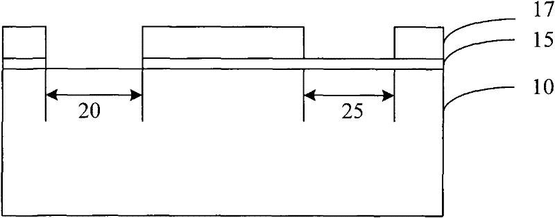
[0038] It can be seen from the background technology that in the prior art, since the field oxygen in the isolation region and the thermal oxide layer in the drift region are formed in the same process, the thickness of the thermal oxide layer in the drift region can only be the same as the thickness of the field oxygen, so that the drift region The thickness of the thermal oxide layer is uncontrollable, and in order to ensure the effect of isolation, the field oxygen usually needs to be thicker. Too thick thermal oxide layer in the drift region will weaken the depletion effect of the drift region, and cannot achieve the best withstand voltage effect. In addition, the implantation of the field region and the implantation of the drift region need to be defined twice by lithography, and one more lithography process increases the cost.

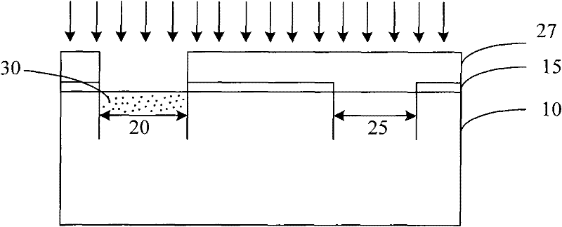
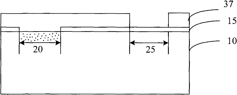
[0039] After a lot of experiments, the inventor of the present invention has obtained a manufacturing method of a semiconductor device by first g...


PUM


Abstract

The invention provides a semiconductor device and a manufacturing method thereof, wherein the manufacturing method comprises the following steps: providing a semiconductor substrate, wherein the semiconductor substrate comprises a hard mask layer which is arranged on the surface of the semiconductor substrate and the semiconductor substrate comprises a first region and a second region; removing the hard mask layer from the surface of the semiconductor substrate in the first region; implanting impurity ions in the first region; growing a first silicon oxide layer on the semiconductor substrate in the first region; removing the hard mask layer from the surface of the semiconductor substrate in the second region; growing a second silicon oxide layer respectively in the first region with the first silicon oxide layer and on the semiconductor substrate in the second region, thus improving the withstand voltage effect of a high voltage device.

Description

technical field [0001] The invention relates to the technical field of semiconductor manufacturing, in particular to a semiconductor device and a manufacturing method thereof. Background technique [0002] High-voltage devices are widely used in modern integrated circuit design. The corresponding high-voltage process needs to provide many types of devices for circuit design, such as high-voltage MOS tubes, low-voltage MOS tubes, resistors, capacitors, inductors, etc. Therefore, the high-voltage process The integration level itself is very high, and the performance requirements for these devices are also very high. The high-voltage devices mentioned here refer to planar high-voltage devices. [0003] Generally, in the high-voltage process above 0.35um, the most commonly used isolation method for high-voltage MOS devices is the LOCOS (Local Oxidation of Silicon) process, that is, a thick oxide film is grown in the area other than the active area as the isolation layer, also kn...

Claims


Application Information

Patent Timeline
Patent Type & Authority Applications(China)
IPC IPC(8): H01L21/762H01L29/78
Inventor 郭立罗泽煌吴孝嘉
Owner CSMC TECH FAB1
Why Eureka
Try Eureka