Method for integrating manganese-oxide-based resistive memory with copper interconnection rear end process

A manganese oxide-based, back-end process technology, which is applied in the field of resistive memory and copper interconnection back-end process integration, can solve the problems of not being able to replace Flash, increase the aspect ratio, increase power consumption, etc., and achieve low manufacturing costs , Reduce power consumption, improve yield and reliability

Inactive Publication Date: 2011-11-09
FUDAN UNIV
View PDF5 Cites 9 Cited by
  • Summary
  • Abstract
  • Description
  • Claims
  • Application Information

AI Technical Summary

Problems solved by technology

Due to the limitation of grain size of Cu, W and other materials, when the corresponding oxides are used as storage media, the leakage current will be large, thereby increasing power consumption, and cannot effectively replace Flash at the 45nm and 32nm stages
And at the 45nm and 32nm process nodes, the thickness of the barrier layer is required to be reduced to 4.9nm and 3.6nm respectively, and the aspect ratio is further increased. Traditional Ti / TiN, Ta / TaN, etc. cannot meet the requirements. Therefore, titanium oxide The application of storage media such as tantalum oxide and tantalum oxide in the back end of copper interconnection will also be limited by the process

Method used


Image

  • Method for integrating manganese-oxide-based resistive memory with copper interconnection rear end process
  • Method for integrating manganese-oxide-based resistive memory with copper interconnection rear end process
  • Method for integrating manganese-oxide-based resistive memory with copper interconnection rear end process

Examples


Embodiment Construction

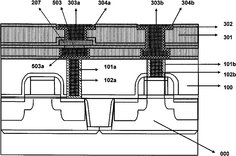
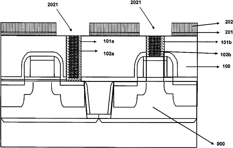
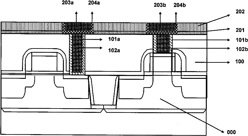
[0043] The invention is described more fully hereinafter in reference to the examples illustrated in the illustrations, providing preferred embodiments but should not be considered limited to the embodiments set forth herein. In the drawings, the thicknesses of layers and regions are exaggerated for clarity, but as schematic diagrams, they should not be considered as strictly reflecting the proportional relationship of geometric dimensions.

[0044] The drawings referenced herein are schematic illustrations of idealized embodiments of the invention, and the illustrated embodiments of the invention should not be considered limited to the particular shapes of the regions shown in the drawings, but include resulting shapes, such as manufacturing-induced deviation. For example, the curves obtained by dry etching usually have curved or rounded characteristics, but in the illustrations of the embodiments of the present invention, they are all represented by rectangles, and the repre...


PUM

PropertyMeasurementUnit
thicknessaaaaaaaaaa
thicknessaaaaaaaaaa
thicknessaaaaaaaaaa

Abstract

The invention belongs to the technical field of semiconductor memories and particularly relates to a method for integrating a manganese-oxide-based resistive memory with a copper interconnection rear end process. In the method for process integration, manganese metal in a cap layer on a copper lead wire is siliconized to form a MnSi compound layer and the MnSi compound layer is oxidized to form aMnSi(x)O(y) storage medium layer; and a manganese silica compound layer is used as a barrier layer of the copper lead wire at a copper interconnection rear end. The method has the advantages of compatibility with the copper interconnection rear end process with process nodes equal to or less than 45 nanometers; and the manganese-oxide-based resistive memory has low preparation cost, high reliability and low power consumption.

Description

technical field [0001] The invention belongs to the technical field of semiconductor memory, in particular to a resistive memory (Resistive Memory) based on a MnSixOy storage medium layer (0.001<x≤2, 2<y≤5), in particular to a resistive memory based on a MnSixOy storage medium layer and copper A method for interconnect back-end process integration. Background technique [0002] Memory occupies an important position in the semiconductor market. Due to the continuous popularization of portable electronic devices, the share of non-volatile memory in the entire memory market is also increasing, and more than 90% of the share is occupied by FLASH (flash memory). However, due to the requirement of storing charges, the floating gate of FLASH cannot be thinned without limit with the development of technology generation. It is reported that the limit of FLASH technology is around 32nm, which forces people to look for the next generation of non-volatile memory with better perfor...

Claims


Application Information

Patent Timeline
Patent Type & Authority Applications(China)
IPC IPC(8): H01L21/82H01L21/768H01L45/00H01L27/24
Inventor 林殷茵田晓鹏
Owner FUDAN UNIV
Why Eureka
Try Eureka