LED preparation method for improving light-emitting efficiency

A technology of light-extraction efficiency and light-emitting layer, applied in electrical components, circuits, semiconductor devices, etc., can solve problems such as difficult contact and reflection effect, improve light-extraction efficiency and yield, and solve the effect of poor adhesion

Active Publication Date: 2011-11-16
LATTICE POWER (JIANGXI) CORP
View PDF5 Cites 17 Cited by
  • Summary
  • Abstract
  • Description
  • Claims
  • Application Information

AI Technical Summary

Problems solved by technology

At the same time, due to the high-energy impact in laser lift-off, it is difficult to make a good contact and reflection effect between the high-reflectivity metal and the GaN P-surface

Method used


Image

  • LED preparation method for improving light-emitting efficiency
  • LED preparation method for improving light-emitting efficiency
  • LED preparation method for improving light-emitting efficiency

Examples


preparation example Construction

[0055] The present invention proposes a LED preparation method for improving light extraction efficiency, which includes:

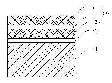
[0056] j. After growing the buffer layer, n-GaN, light-emitting layer, and p-GaN epitaxial film successively on the sapphire substrate, evaporate the transparent conductive layer and perform alloy treatment to grow the SiO2 protective layer;

[0057] k. Apply the adhesive to the SiO2 protective layer and cure it together with the temporary support substrate;

[0058] l. Laser lift off the sapphire substrate;

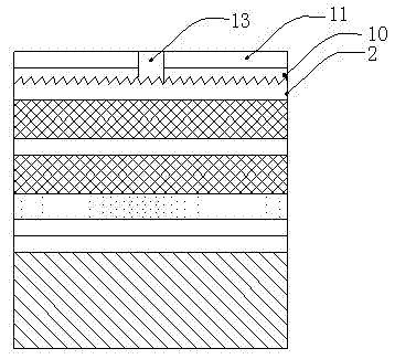
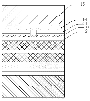
[0059] m. Roughen the N face of the peeled epitaxial film;

[0060] n. Make a transparent, curable adhesive material layer on the N side of the epitaxial film, and cure the adhesive material layer;

[0061]o. prepare the reflective layer, and carry out high-temperature curing together with the above-mentioned bonding material layer;

[0062] p. Form electrode-shaped electrode grooves on the layer above the roughened surface, and make N electrodes...

Embodiment 3

[0073] Embodiment three of the present invention. The steps of this example are basically the same as those of Example 2. Compared with the second embodiment, the temporary support substrate of this example is made of sapphire. Embodiment three is briefly described as follows:

[0074] After the buffer layer, n-GaN, light-emitting layer, p-GaN and other thin films are grown sequentially on the sapphire substrate by MOCVD, ITO is evaporated and treated with a 500-degree alloy. Apply the adhesive to the ITO layer protected by SiO2, and bond it to the temporary support sapphire substrate, cure at 100 degrees for 60 minutes, Kr laser, power 500mW, and perform laser peeling of the sapphire surface. After the sapphire is peeled off, the gallium nitride surface is cleaned and roughened with an alkaline solution (KOH solution) at 80 degrees; the water glass is applied to the roughened gallium nitride surface, and then cured at 80 degrees for 15 minutes. The thickness of the transpa...


PUM


Abstract

The invention relates to a light-emitting diode (LED) preparation method for improving light-emitting efficiency and relates to a preparation process for a semiconductor luminescent device. The method aims to improve the light-emitting efficiency and the yield of products. In the technical scheme, the preparation method comprises the following steps of: allowing an epitaxy membrane to grow on a sapphire substrate, and performing vapor deposition and alloying on a transparent conducting layer to grow a SiO2 protective layer; coating mucilage glue on the SiO2 protective layer, and curing with a temporary support baseplate; stripping the sapphire substrate by laser; coarsening the N surface of the stripped epitaxy membrane; manufacturing a transparent bonding material layer capable of being cured on the N surface of the stripped epitaxy membrane, and curing the bonding material layer; preparing a reflective layer, and curing with the bonding material layer at high temperature; manufacturing an N electrode in a groove formed on a layer on the coarsened surface; evaporating a bonding metal layer, and performing eutectic bonding with a conducting and heat-conducting perpetual baseplate; and removing the temporary support baseplate and the SiO2 protective layer, and manufacturing a P electrode on the transparent conducting layer.

Description

technical field [0001] The invention relates to a preparation process of a semiconductor light emitting device. Background technique [0002] The sapphire substrate is the main substrate for GaN-based LED epitaxial growth, and its conductivity and heat dissipation are relatively poor. After removing the sapphire substrate by laser lift-off technology, the LED is made into a vertical structure, which can effectively solve the heat dissipation and light emission problems. . The usual practice is to use the GaN N surface to emit light, and look for reflectors and protective layer metals that match the P surface. However, the use of laser to lift off the sapphire substrate, the current low yield has been the bottleneck of the industrialization of GaN-based LED thin film chips. Due to the stress caused by the difference in thermal expansion coefficient between sapphire, GaN film and support substrate, or the poor adhesion between reflective metal and GaN P surface, the GaN fil...

Claims


Application Information

Patent Timeline
Patent Type & Authority Applications(China)
IPC IPC(8): H01L33/00
Inventor 陈栋赵汉民周印华
Owner LATTICE POWER (JIANGXI) CORP
Why Eureka
Try Eureka