

Power circuit
A power supply circuit and circuit technology, applied in electrical components, regulating electrical variables, instruments, etc., can solve the problems of not considering the temperature drift and parameter discreteness of other devices, unadjustable temperature compensation parameters, and inability to withstand high voltage input. Modular design and optimization, large input voltage fluctuation range, good independence and the effect of flexibility
- Summary
- Abstract
- Description
- Claims
- Application Information
AI Technical Summary
Problems solved by technology
Method used
Image


Examples
Embodiment 1
[0136] In this embodiment, the structure of the power supply circuit is as follows Figure 2b As shown, the RTD adopts Pt1000 (zero-degree resistance 1k ohms), and the adjustable parameter constant current source adopts Figure 3a , Figure 3b The two structures, and use the variable resistor R0 to adjust the current I0. Figure 3a It is based on the JFET structure, because the reverse saturation conduction current I0=Idss of the JFET is relatively small, generally around tens of uA to several mA, when the amplification factor of the adjustment tube T1 is relatively large (such as using Darlington Tube), can realize low power consumption design; Figure 3b Based on the structure of the transistor, the current I0 is adjusted by the resistor R0, and the range can be tens of uA to tens of mA, which can directly realize the driving of the high-power tube T1. JFET can also be replaced by VMOS tube to achieve the same low power consumption and high power driving effect, but becau...
Embodiment 2
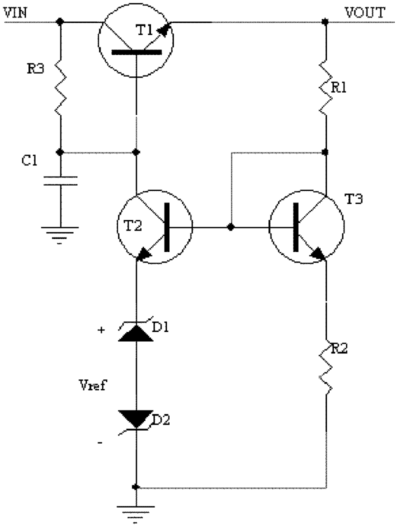
[0147] In this embodiment, the structure of the power supply circuit is as follows Figure 6a As shown, the difference between embodiment two and embodiment one is mainly:
[0148] NPN tube T1 is used to bias the ground to drive PNP tube T3 as a voltage adjustment circuit to achieve a low dropout (within 1.0V) and low output voltage (about 2.4V) structure, and greatly reduce the base current I1 of T1 to constant The diversion effect of the flow source I0;
[0149] Among them, the temperature compensation Rt1 for Vref adopts Pt100 with a smaller resistance value (zero-degree resistance 100 ohms);
[0150] If the power consumption is too large, or the temperature compensation range of Rt is not enough, the output sampling voltage divider resistors R1 and R2 (that is, the bias resistor Rt2 of T2) also use PTC or NTC thermistors for further compensation to improve the power supply. Accuracy and temperature adaptation range.
[0151] The production and debugging process of the p...
Embodiment 3
[0153] In this embodiment, the structure of the power supply circuit is as follows Figure 6b As shown, it can be considered that the corresponding Figure 2b The T1 adopts the structure of a Darlington tube, and the difference between the third embodiment and the first embodiment is mainly:
[0154] Figure 6b NPN tube T1 is used to bias the output terminal and PNP (or IGBT) tube T3 is used as a voltage adjustment circuit to achieve low power consumption (power consumption mainly depends on I0 of the adjustable parameter constant current source) and low output voltage structure. And greatly reduce the shunting effect of the base current I1 of T1 on the constant current source I0;
[0155] Among them, the temperature compensation Rt1 for Vref adopts Pt1000 with a larger resistance value (zero-degree resistance 1k ohm);
[0156] The voltage dividing resistors R1 and R2 for output sampling (that is, the bias resistor of T2) are also further compensated by PTC or NTC thermisto...
PUM
 Abstract
Description
Claims
Application Information