High-power semiconductor laser array mask device

A laser array and semiconductor technology, applied in ion implantation plating, metal material coating process, coating and other directions, can solve the problems of uneven solder smear, smear dislocation, poor device stability and reliability, etc., and achieve low production costs. , Improve the service life, improve the yield and the effect of service life

Inactive Publication Date: 2011-11-23
CHANGCHUN INST OF OPTICS FINE MECHANICS & PHYSICS CHINESE ACAD OF SCI
View PDF3 Cites 11 Cited by
  • Summary
  • Abstract
  • Description
  • Claims
  • Application Information

AI Technical Summary

Problems solved by technology

[0003] The present invention solves the problem of poor stability and reliability of the device due to the manual application of manual application for the heat sink welding of the insulating sheet and the chip of the device of the existing high-power semiconductor laser array. , providing a high-power semiconductor laser array mask device

Method used


Image

  • High-power semiconductor laser array mask device
  • High-power semiconductor laser array mask device

Examples


specific Embodiment approach 2

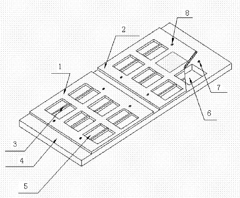
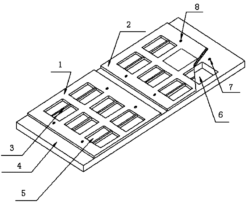
[0013] Specific implementation mode 2. This implementation mode is an application example of the high-power semiconductor laser array mask device described in specific implementation mode 1:

[0014] In this embodiment, the solder on the insulating sheet of the high-power semiconductor laser array is realized by the mask device of the present invention. The mask device needs to evaporate the solder in a vacuum chamber, and the evaporation process is completed in a high-vacuum vacuum chamber.

[0015] The process of using the mask device according to the present invention is as follows: first, place the cleaned first mask plate on the left side of the mask frame; align the 4 symmetrical screw holes, and fix the 4 symmetrical screw holes on the left side with screws. Screw holes, while fixing the screws, observe under the microscope and adjust the square hole of the mask frame to align with the square hole of the mask plate, then place the cleaned mask plate b on the right side o...


PUM


Abstract

The invention relates to a high-power semiconductor laser array mask device, belonging to the technical field of electronics. The invention solves the problems of low stability and reliability of the device since the welding flux can be easily spread unevenly and dislocated when the heat sink welding of the insulating piece and chip of the high-power semiconductor laser array device adopts manual spreading. The high-power semiconductor laser array mask device comprises a first mask board, a second mask board, a mask strip and a mask board frame, wherein the first mask board and the second mask board are respectively fixed to the mask board frame, and respectively provided with six mask board square hole groups; each mask board square hole group is evenly divided into two mask board square holes by the mask strip; two mask board frame square hole groups are arranged in the mask board frame; and each mask board frame square hole group is provided with six mask board frame square holes which are symmetrical with the first mask board and the second mask board. The device is simple and practical, has the advantages of low manufacturing cost, favorable consistency and high welding flux spreading precision, and is suitable for manufacturing high-power semiconductor laser arrays.

Description

technical field [0001] The invention relates to the technical field of semiconductor optoelectronics, in particular to a high-power semiconductor laser array mask device. Background technique [0002] At present, most domestic high-power semiconductor laser array insulation sheets and chip heat sinks are welded manually. Manual operation is that the operator uses a special smear tool to smear the solder on the insulating sheet under the microscope. During the smearing process, it is easy to have too much solder; Cause the upper and lower electrodes short circuit and so on. The device stability, reliability, lifetime and yield of the array of high-power lasers are seriously affected. The array device welded by this jig greatly reduces the cost and improves the efficiency of the array device welding process. Therefore, in order to obtain a high-stability, high-reliability, and high-power semiconductor excitation array device, it is necessary to use a simple and practical, lo...

Claims


Application Information

Patent Timeline
Patent Type & Authority Applications(China)
IPC IPC(8): C23C14/04C23C14/24
Inventor 刘云王立军宁永强秦莉单肖楠付喜宏张金龙
Owner CHANGCHUN INST OF OPTICS FINE MECHANICS & PHYSICS CHINESE ACAD OF SCI
Why Eureka
Try Eureka