A kind of semiconductor power device and its manufacturing method

A technology for power devices and semiconductors, which is used in the manufacture of semiconductor/solid-state devices, semiconductor devices, transistors, etc., and can solve the problem of increased possibility of channel region punch-through under drain-source reverse bias and reduced channel region doping concentration, etc. problem, to achieve the effect of low Rds, lower Rds, and higher breakdown voltage

Inactive Publication Date: 2011-11-30
FORCE MOS TECH CO LTD
View PDF2 Cites 10 Cited by
  • Summary
  • Abstract
  • Description
  • Claims
  • Application Information

AI Technical Summary

Problems solved by technology

[0004] In addition, there is another disadvantage in this prior art: since both the n+ doped region and the p-type body region are formed before the trench gate, when the cell density of the device exceeds 112 million cells per square inch (that is, the device When the cell pitch is reduced to 2.4 microns), the punch-through problem is almost inevitable
Boron accumulated near the channel region will lead to a decrease in the doping concentration of the channel region, which in turn increases the possibility of channel region punch-through under reverse bias of the drain source

Method used


Image

  • A kind of semiconductor power device and its manufacturing method
  • A kind of semiconductor power device and its manufacturing method
  • A kind of semiconductor power device and its manufacturing method

Examples


Embodiment Construction

[0049] The invention is explained in more detail below with reference to the accompanying drawings, in which preferred embodiments of the invention are shown. The present invention can be embodied in different ways and should not be limited to the embodiments described herein. For example, the description here refers more to N-channel MOSFET devices, but clearly other devices are also possible.

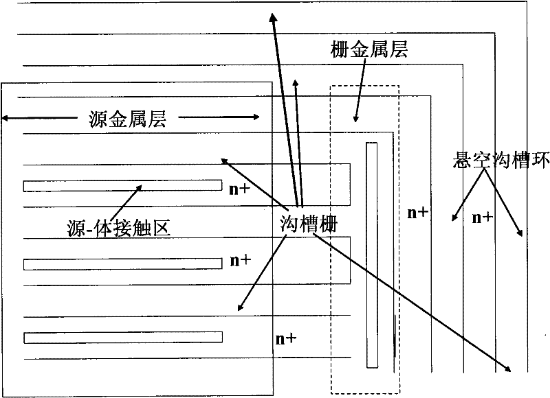
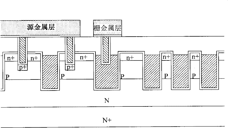
[0050] refer to Figure 2A and 2B A sectional view and a top view of a preferred embodiment according to the present invention are shown respectively. In this embodiment, an N-channel MOSFET device 100 is formed on an N+ substrate 105 and has an N-type epitaxial layer 110 . The MOSFET device includes a trench gate 120 within a trench whose inner surface is lined with a gate insulating layer 115 . The P-type body region 125 is located between the trench gates 120 , and the P-type body region 125 includes an N+ source region 130 close to the upper surface of the P-type body region 1...


PUM


Abstract

The invention discloses a trench metal oxide semiconductor field effect transistor device, which comprises a plurality of closed trench metal oxide semiconductor field effect transistor units surrounded by trench gates, forming a square or rectangular pattern in the active region. Closed cell structure. And in the terminal area of ​​the device, multiple trench rings with floating voltage are included to improve the breakdown voltage of the device.

Description

technical field [0001] The invention relates to a unit structure of a semiconductor power device, a device structure and a manufacturing method. In particular, it relates to a novel cell structure, device structure and improved manufacturing method of a trench metal oxide semiconductor field effect transistor. Background technique [0002] As the cell density of semiconductor power devices increases, new device structures are urgently needed to reduce source-drain resistance (Rds). At the same time, in order to make semiconductor power devices have a wider application range, the reduction of Rds cannot be at the expense of sacrificing the reliability of the device and reducing the breakdown voltage. Conventional design techniques and device structures become extremely challenging to meet the above requirements, especially as the cell density of semiconductor power devices exceeds 600 million per square inch. [0003] In U.S. Patent No. 6,462,376, a DMOS (double-diffused me...

Claims


Application Information

Patent Timeline
Patent Type & Authority Applications(China)
IPC IPC(8): H01L27/088H01L27/092H01L29/06H01L21/8234H01L21/8238
Inventor 谢福渊
Owner FORCE MOS TECH CO LTD
Why Eureka
Try Eureka