A technology to improve the conversion efficiency of solar photovoltaic cells
A photovoltaic cell, conversion efficiency technology, applied in the direction of photovoltaic power generation, circuits, electrical components, etc., can solve the problem that the "dead layer" area cannot be completely eliminated
- Summary
- Abstract
- Description
- Claims
- Application Information
AI Technical Summary
Problems solved by technology
Method used
Image
Examples
Embodiment Construction
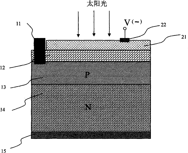
[0012] Attached below figure 2 , a schematic diagram of a P-N junction (P on N) solar photovoltaic cell of Si semiconductor material, specifically illustrating an embodiment of the present invention. The examples are only for illustrating the present invention, and should not be construed as limiting the scope and spirit of the present invention.
[0013] Such as figure 2 :
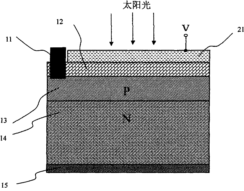
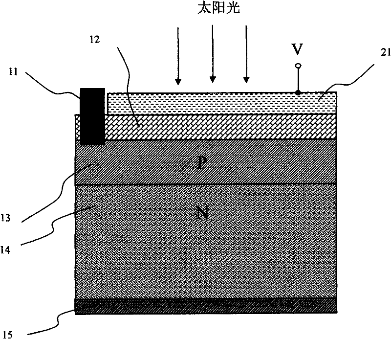
[0014] Embodiment: 11 and 15 are output electrodes of solar photovoltaic cells, 12 is dense and pinhole-free SiO 2 Transparent insulating dielectric mask mask layer, 13 and 14 are the P-N junction of Si semiconductor. In SiO 2 On the mask layer 12 of the transparent insulating dielectric mask, a transparent conductive thin film layer 21 of indium tin oxide (ITO) and a contact electrode 22 of the transparent conductive thin film layer are deposited. The transparent conductive film layer 21 and SiO 2 The thickness of the transparent insulating dielectric mask layer 12 should be adjusted so as to mee...
PUM
 Abstract
Description
Claims
Application Information


