
A kind of sapphire substrate surface order roughening method and sapphire substrate, led preparation method and led

A technology of sapphire and patterned sapphire, applied in nanotechnology, electrical components, nanotechnology, etc. for materials and surface science, can solve the problems of reducing dislocations, time-consuming process, high production cost, etc., to promote scattering and performance Excellent, the effect of large quantity per unit area

Inactive Publication Date: 2011-12-14
INST OF MECHANICS - CHINESE ACAD OF SCI
View PDF6 Cites 8 Cited by
  • Summary
  • Abstract
  • Description
  • Claims
  • Application Information

AI Technical Summary

Problems solved by technology

The current method of preparing photonic crystals is mainly the traditional EBL (Electron Beam Etching), which has high production costs and low efficiency.
[0004] Using lateral epitaxy technology can significantly reduce dislocations, but the two-step growth process is time-consuming in process

Method used


Image

  • A kind of sapphire substrate surface order roughening method and sapphire substrate, led preparation method and led
  • A kind of sapphire substrate surface order roughening method and sapphire substrate, led preparation method and led
  • A kind of sapphire substrate surface order roughening method and sapphire substrate, led preparation method and led

Examples


Embodiment Construction

[0037] The method for the orderly roughening of the surface of the sapphire substrate of the present invention is specifically:

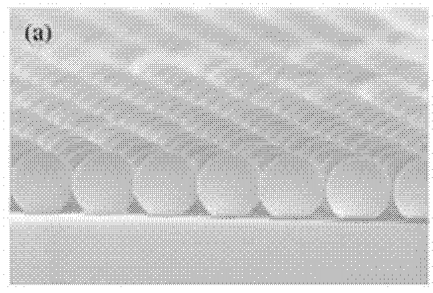
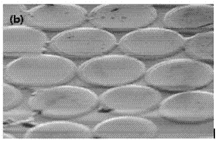
[0038] Such as figure 1 As shown, firstly, the polystyrene nanospheres are evenly distributed on the surface of the sapphire substrate. The uniform distribution methods include: 1. The LB film method, that is, the polystyrene micro-nanospheres are spread on the water or oil / water interface by self-assembly ; 2, spin-coating (spin-coating method), the polystyrene microsphere emulsion is added dropwise on the substrate, and the spin coating is carried out by using a homogenizer; 3, the vertical sheet pulling self-assembly method, the substrate is inserted into a certain concentration (0.01-1%) polystyrene microsphere solution, and then pulled at a constant speed (10 μm / s-1 cm / s) to form a film.

[0039] Then the sapphire substrate is placed in a Cl-BCl mixed atmosphere, etched with an ICP etching machine, and two-dimensional ordered patterns are prep...


PUM

PropertyMeasurementUnit
Diameteraaaaaaaaaa
Diameteraaaaaaaaaa

Abstract

The invention discloses a method for orderly roughening the surface of a sapphire substrate, comprising the following steps: Step 1, uniformly distributing polystyrene nanospheres on the surface of a sapphire substrate; In the atmosphere, use an ICP etching machine to etch; step 3, remove the polystyrene nanospheres, so as to obtain a patterned sapphire substrate with small protrusions evenly distributed on the surface. The invention also discloses a sapphire substrate, a preparation method of the LED and the LED. In the present invention, polystyrene nanospheres with a certain diameter are formed on the sapphire substrate, and the nanospheres are ordered and evenly distributed on the surface of the substrate, and then etched to form nanoscale patterns on the surface of the substrate. Ordered small protrusions, the diameter, spacing and height of the small protrusions can be 550nm, 60nm and 150nm respectively. Therefore, the number of protrusions per unit area formed by the present invention is more, which can promote light scattering, thereby obtaining LEDs with better performance.

Description

technical field [0001] The invention relates to a method for orderly roughening the surface of a sapphire substrate, a sapphire substrate, an LED preparation method and the LED. Background technique [0002] At present, GaN photodiodes (LEDs) with high light extraction efficiency have good applications in many places, such as traffic lights, full-color displays, liquid crystal display background light sources, and solid-state lighting. However, there are a large number of dislocations in the epitaxial GaN layer based on the sapphire substrate, as well as the mismatch between the thermal expansion coefficients of the two, which will reduce the intrinsic quantum efficiency of the LED. Moreover, due to the large difference in refractive index between the GaN layer and air, internal total reflection will limit the light extraction efficiency. Therefore, in order to improve the light extraction efficiency, it is necessary to improve the intrinsic quantum efficiency and light ext...

Claims


Application Information

Patent Timeline
IPC IPC(8): H01L33/00H01L33/22B82Y30/00B82Y40/00
Inventor 蓝鼎王育人
Owner INST OF MECHANICS - CHINESE ACAD OF SCI
Learn More