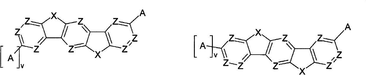
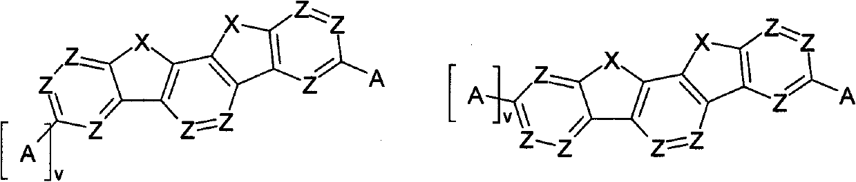
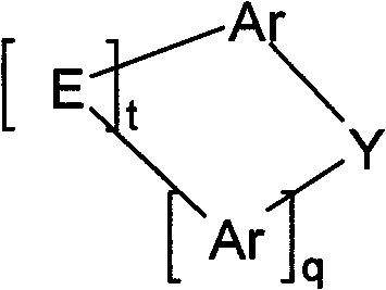
Materials for Organic Electroluminescent Devices
A technology of general formula and compound, applied in the field of materials for organic electroluminescent devices, can solve the problems of low efficiency, blocking vapor deposition source, difficult realization, etc.
- Summary
- Abstract
- Description
- Claims
- Application Information
AI Technical Summary
Problems solved by technology
Method used
Image

Examples
Embodiment 1
[0146] a) Synthesis of thioethers
[0147]
[0148] 200g (732mmol) 2-bromo-9,9-dimethyl-9H-fluorene, 122.9g (732mmol) 2-methylsulfanylphenylboronic acid and 202g (950mmol) K 2 CO 3 Suspended in 850ml THF and 850ml water, the mixture was washed with N 2 After saturation, 3.3 g (2.9 mmol) of tetrakis(triphenylphosphine)palladium(0) were added and the mixture was heated at the boil for 2 hours. The mixture was poured into 3 L of a 1:1:1 mixture of water / MeOH / 6M HCl, the beige precipitate was filtered off with suction, washed with water and dried. according to 1 The product content determined by H-NMR was about 95%, and the total yield was 190 g (82%).
[0149] b) oxidation
[0150]
[0151] First 196 g (619.3 mmol) of the compound from a) were introduced under protective gas into 2.3 L of glacial acetic acid and 250 ml of dichloromethane and cooled to 0°C. To this solution was added dropwise 1.1 L (619 mmol) of 30% H 2 o 2 solution, and the mixture was stirred overn...
Embodiment 2-9
[0161] Examples 2-9: Fabrication of OLEDs
[0162] The inventive OLEDs are produced by the general method according to WO 04 / 058911, which is adapted to the conditions described here (layer-thickness variation, materials used).
[0163] Results for various OLEDs are given in Examples 2 to 9 below. A glass plate coated with structured ITO (indium tin oxide) forms the matrix of the OLED. For improved processing, 20 nm of PEDOT (poly(3,4-ethylenedioxy-2,5-thiophene), applied by spin coating from water, purchased from H.C. Starck, Goslar, Germany) was applied to the substrate superior. The OLED consists of the following sequential layers: substrate / PEDOT 20nm / HIL1 5nm / hole transport layer (HTM) 20, 110 or 200nm / NPB 20nm / emissive layer (EML) 30 or 40nm / electron transport layer (ETM) 20nm and finally of the cathode.
[0164] Materials other than PEDOT were applied by thermal vapor deposition in a vacuum chamber. The emitting layer here always consists of a matrix material (host...
PUM
| Property | Measurement | Unit |
|---|---|---|
| Thickness | aaaaa | aaaaa |
| Thickness | aaaaa | aaaaa |
Abstract
Description
Claims
Application Information