Substrate for electronic device and electronic device using the same
A technology for electronic devices and substrates, which is applied in the field of substrates for electronic devices to achieve the effect of high effective area and suppression of short circuit between electrodes
- Summary
- Abstract
- Description
- Claims
- Application Information
AI Technical Summary
Problems solved by technology
Method used
Image
Examples
no. 1 approach
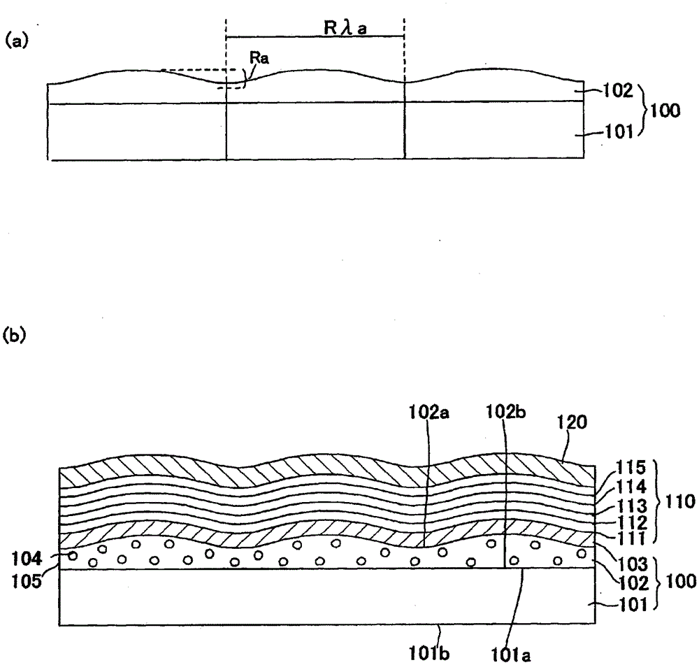
[0113] Hereinafter, the substrate for an electronic device (translucent substrate with electrodes) and the organic LED element according to the first embodiment of the present invention will be described with reference to the drawings. figure 1 (a) is a substrate for an electronic device according to the first embodiment of the present invention, figure 1 (b) is a cross-sectional view showing the structure of an organic LED element having the substrate for electronic devices.
[0114] The electronic device substrate for forming the organic LED element of the present invention, such as figure 1 As shown in (a), it is characterized by having a glass substrate 101 and a scattering layer 102 including a glass layer formed on a surface 101a on the first main surface side of the glass substrate 101, and the scattering layer 102 has a The second surface 102b that is in contact with the surface 101a on the first main surface side and the first surface 102a that is opposite to the second su...
no. 2 approach
[0331] (Other structural examples of organic LED elements)
[0332] Hereinafter, the structure of the substrate for an electronic device and the organic LED element of the second embodiment of the present invention will be described using the drawings. In addition, for figure 1 The same structure is marked with the same number, and the description is omitted. Figure 23 It is a cross-sectional view showing another structure of the translucent substrate for an organic LED element of the present invention and an organic LED element formed using the substrate. Another organic LED element of the present invention is composed of a translucent substrate 1400 with translucent electrodes, an organic layer 1410, and a reflective electrode 120. The translucent substrate 1400 with translucent electrodes is composed of a translucent substrate 101, a scattering layer 1401, and a translucent electrode 103. The organic layer 1410 is composed of a hole injection / transport layer 1411, a light em...
Embodiment
[0337] (Verification of the effect of the scattering layer)
[0338] Hereinafter, the verification process that the scattering layer is effective for improving the light extraction efficiency will be explained. Sample 1 is an example provided with the undulating scattering layer of the present invention, and sample 2 is a comparative example provided with a scattering layer in which no scattering material is provided. The calculation method is the same as the calculation method of the scattering layer described above. Below, the conditions and results (front extraction efficiency) are listed in Table 2.
[0339] Table 2
[0340]
Sample 1
Sample 2
Electron injection / transport layer
Thickness (μm)
1
1
1.9
1.9
Luminescent layer
Thickness (μm)
1
1
1.9
1.9
Hole injection / transport layer
Thickness (μm)
1
1
1.9
1.9
Scattering layer
Substrate
Thickness (μm)
30
30
[0341] Refractive index
1.9
1....
PUM
| Property | Measurement | Unit |
|---|---|---|
| surface roughness | aaaaa | aaaaa |
| surface roughness | aaaaa | aaaaa |
| glass transition temperature | aaaaa | aaaaa |
Abstract
Description
Claims
Application Information


