Thin film solar cell module and manufacturing method thereof
A technology for solar cells and thin films that can be used in final product manufacturing, sustainable manufacturing/processing, circuits, etc., and can solve problems such as the introduction of pollutants
- Summary
- Abstract
- Description
- Claims
- Application Information
AI Technical Summary
Problems solved by technology
Method used
Image

Examples
Embodiment Construction
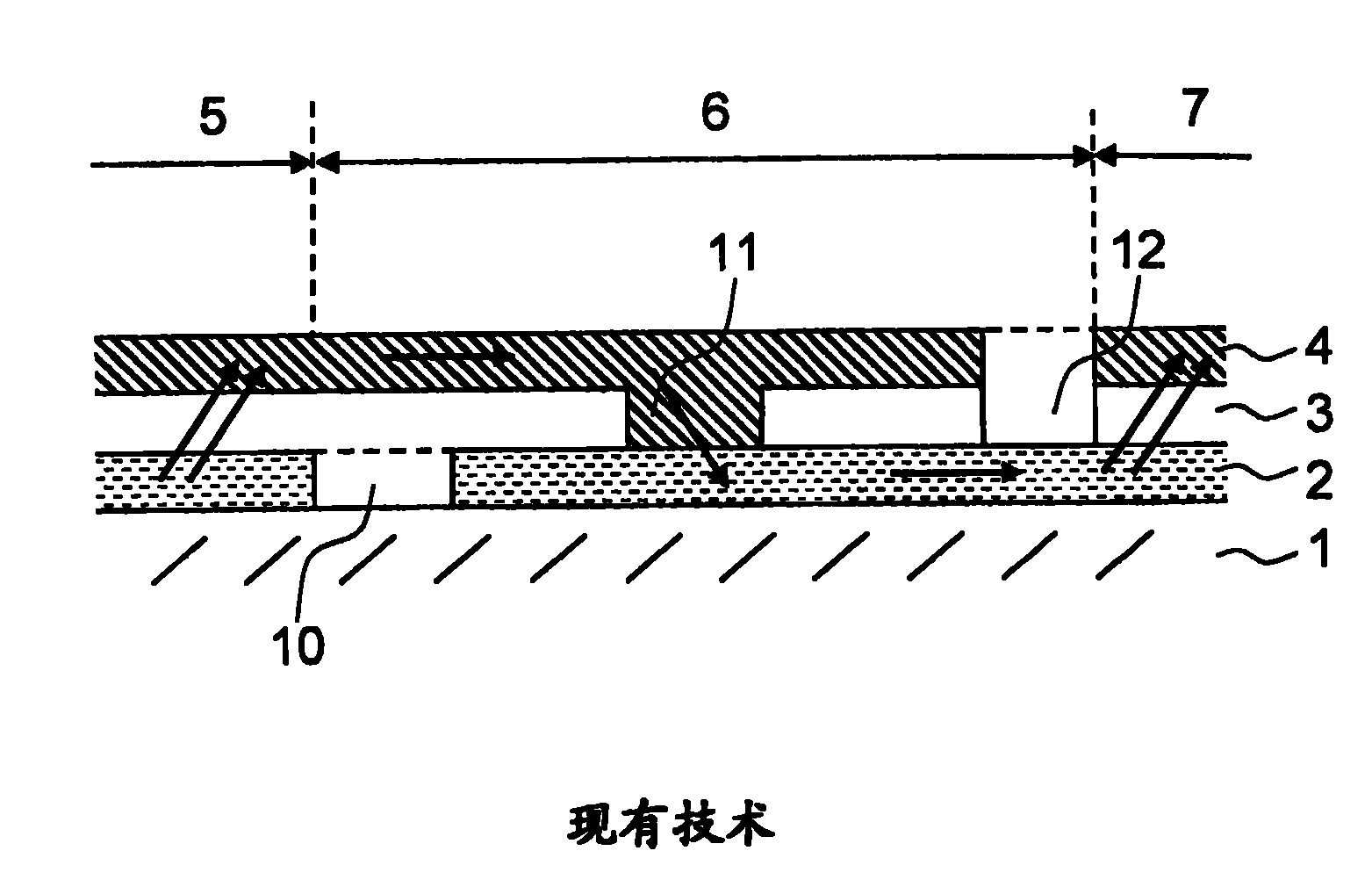
[0027] figure 1 The layer structure of a thin-film solar cell module according to the prior art is shown schematically. A first electrode 2 , a photosensitive layer sequence 3 and a second electrode 4 are applied to the substrate 1 . The first electrode 2 , the photoactive layer sequence 3 and the second electrode 4 are interrupted laterally by separating lines 10 , 11 , 12 . Three separation lines 10, 11, 12 are laterally spaced from each other on their sides and divide the shown part of the thin-film solar cell module into a first segment 5 to the left of the separation line 10, a second segment 7 to the right of the separation line 12, and a The contact area 6 in between.
[0028] Usually, the electrodes 2 , 4 and the photoactive layer sequence 3 in thin-film solar cell modules are applied in a vacuum process. For this, PVD (Physical Vapor Deposition) processes such as plasma sputtering or electrode beam evaporation, or CVD (Chemical Vapor Deposition) processes such as L...
PUM
 Abstract
Description
Claims
Application Information
 - R&D
- Intellectual Property
- Life Sciences
- Materials
- Tech Scout
- Unparalleled Data Quality
- Higher Quality Content
- 60% Fewer Hallucinations
Browse by: Latest US Patents, China's latest patents, Technical Efficacy Thesaurus, Application Domain, Technology Topic, Popular Technical Reports.
© 2025 PatSnap. All rights reserved.Legal|Privacy policy|Modern Slavery Act Transparency Statement|Sitemap|About US| Contact US: help@patsnap.com