Novel LED packaging structure

A technology of LED packaging and LED chips, applied in electrical components, electrical solid devices, circuits, etc., can solve problems such as uneven light spots, low light extraction efficiency, and uneven color temperature, and achieve improved uniformity, light output efficiency, and high color temperature consistent effect

Inactive Publication Date: 2012-01-04
SHENZHEN GLORY SKY OPTOELECTRONICS CO LTD
View PDF5 Cites 8 Cited by
  • Summary
  • Abstract
  • Description
  • Claims
  • Application Information

AI Technical Summary

Problems solved by technology

[0003] In view of the technical problems existing in the prior art such as fast LED light decay, uneven light spots, unbalanced color temperature, and low light extraction efficiency, the purpose of the present invention is to provide a LED with small light decay, good uniformity of light spots, balanced color temperature, and high light output efficiency. The new LED package structure

Method used


Image

  • Novel LED packaging structure
  • Novel LED packaging structure
  • Novel LED packaging structure

Examples


Embodiment Construction

[0021] In order to further elaborate on the technical solutions of the present invention, the following will be described in detail in conjunction with the accompanying drawings.

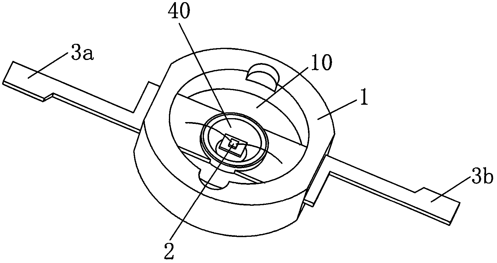
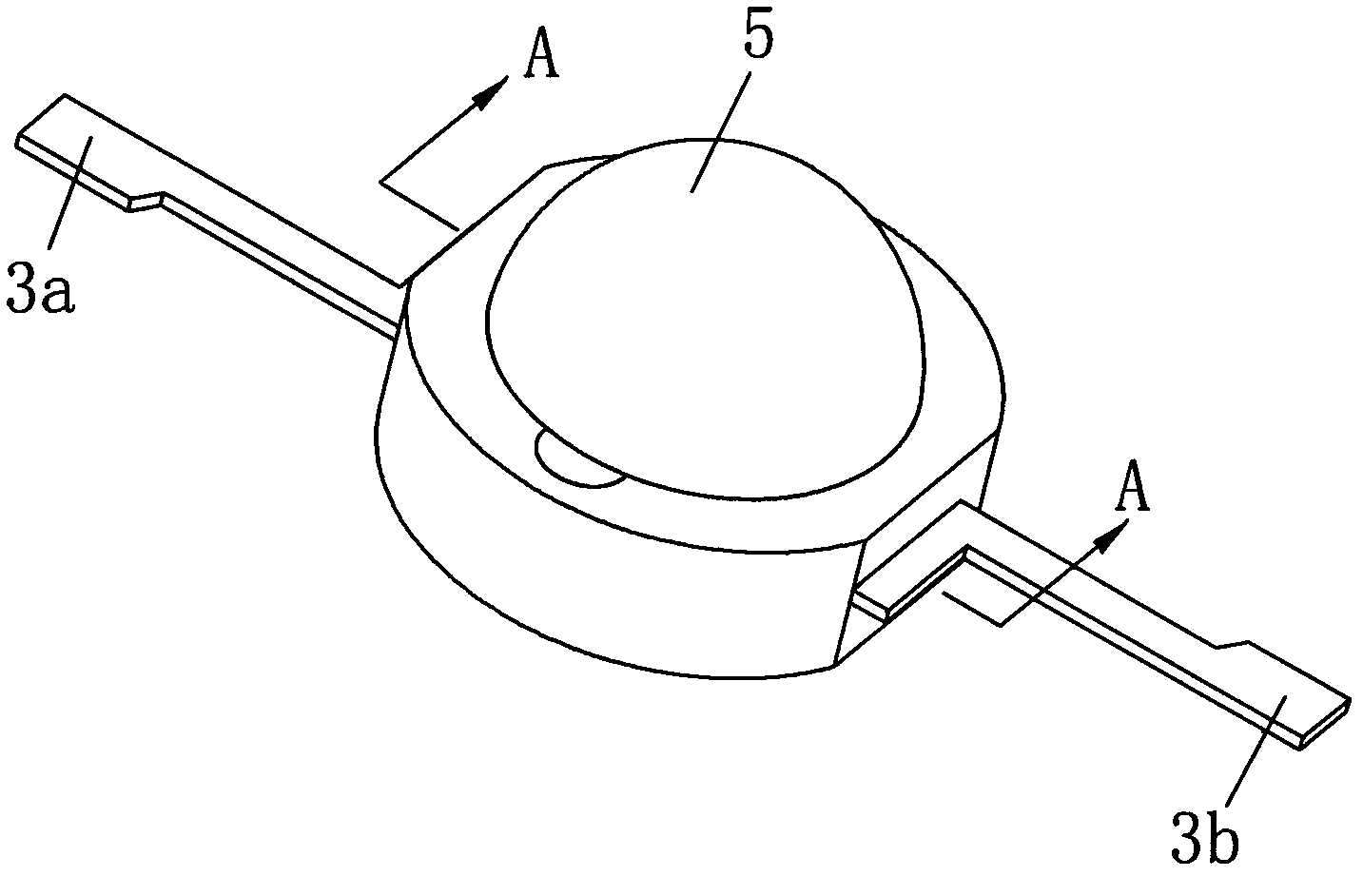
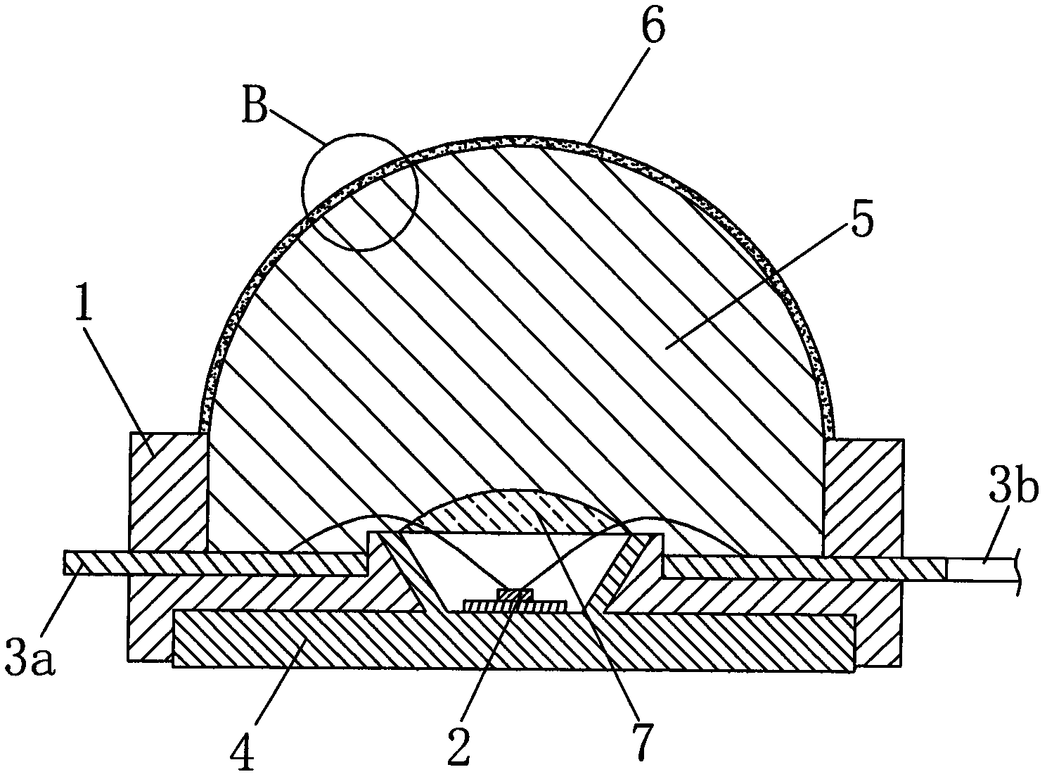
[0022] Such as figure 1 , figure 2 , image 3 As shown, a new LED packaging structure includes a base 1, a cavity 10 formed in the base 1, a heat sink 4 fixed in the cavity 10, a cup and bowl 40 formed on the heat sink 4 and fixed on the The LED chip 2 in the cup bowl 40, a pair of conductive pins 3a, 3b are extended and fixed in the base 1, the LED chip 2 is electrically connected with the conductive pins 3a, 3b, and a lens 5 is formed on the base 1 The LED chip 2 and part of the conductive feet are covered, and a layer of phosphor coating 6 is provided on the outer surface of the lens 5 .

[0023] The LED packaging structure of the present invention breaks the traditional LED packaging mode, and directly transfers the phosphor coating from the original chip surface to the lens surface, so that...


PUM


Abstract

The invention discloses a novel light emitting diode (LED) packaging structure. The structure comprises: a pedestal; a recessed cavity, which is formed in the pedestal; a heat sink, which is fixed in the recessed cavity; a cup bowl, which is formed on the heat sink; and an LED chip, which is fixed in the cup bowl. Besides, a pair of conductive feet are extended and are fixed in the pedestal; the LED chip is electrically connected with the conductive feet; a lens is formed on the pedestal and enables the LED chip and a part of conductive feet to be sealedly capped; and an external surface of the lens are provided with a layer of phosphor coating. According to the LED packaging structure provided in the invention, a traditional LED packaging mode is broken; a phosphor coating is directly transferred from an original chip surface to a surface of a lens, so that the phosphor coating is thoroughly far away from an LED chip and a luminous decay is substantially reduced; moreover, a shape and a thickness of the phosphor coating can be controlled accurately and an excitation area of the phosphor coating can be enlarged, so that an occurrence of a yellow ring can be avoided, a light extraction efficiency is improved and color temperatures of the phosphor coating are highly consistent.

Description

【Technical field】 [0001] The invention relates to an LED structure, in particular to a white light LED packaging structure. 【Background technique】 [0002] Light Emitting Diode (LED) has the characteristics of power saving, light weight and long life. At present, it has achieved the goals of high brightness, multi-color and high luminous efficiency. There are many market changes. In flat panel display products, LED has become the main application market for mobile phone backlight. In the future, LED will be the main axis of development towards large-size flat panel display backlight. Luminous efficiency is the goal of efforts. At present, white light-emitting diode is a kind of light-emitting diode widely used in the lighting field. It excites the fluorescent package mixed with phosphor powder to emit light through the monochromatic light emitted by the chip to generate white light. The traditional package structure of white light-emitting diode is to directly integrate the...

Claims


Application Information

Patent Timeline
Patent Type & Authority Applications(China)
IPC IPC(8): H01L33/50
CPCH01L2224/48091
Inventor 卢志荣黄勇智李兰军
Owner SHENZHEN GLORY SKY OPTOELECTRONICS CO LTD
Why Eureka
Try Eureka