
Patsnap Eureka
For R&D, Patsnap Eureka makes reading and utilizing patents & technical documents easy.
Patsnap Eureka AIR
Designed for self-driven R&D workflows. Generate viable solutions, solve complex R&D challenges, empower your innovation with AI.

Patsnap Eureka Materials
Designed for material experts only. Revolutionize your material R&D, from search, analyze, to developing new materials.

TechResearch
Generate reliable direction feasibility study reports for your R&D in just a few steps.

TechSeek
Discover and master advanced knowledge NOW. Basics, ideas, possibilities, all at once.

TechMind
As an expert in R&D Theories, TechMind can generates customized viable solutions instantly.

TechRisk
Analyze your overall solution with one click, know your potential R&D risks in advance.

TechMonitor
Get weekly tech updates, stay abreast of the latest tech innovations and key insights.
Solid-state imaging apparatus and imaging system
A technology of solid-state imaging and equipment, which is applied in the components of TV systems, image communication, electric solid-state devices, etc., to achieve the effect of reducing actual capacitance
- Summary
- Abstract
- Description
- Claims
- Application Information
AI Technical Summary
Problems solved by technology
Method used
Image

Examples
Embodiment Construction
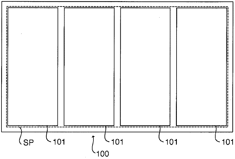
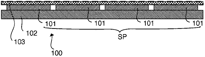
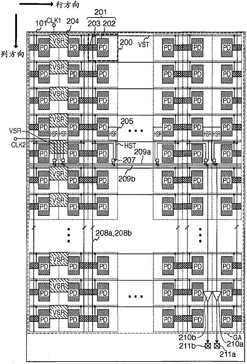
[0023] will refer to Figure 1A with Figure 1B A schematic arrangement of the solid-state imaging device 100 according to an embodiment of the present invention is described. The solid-state imaging device 100 can be formed by, for example, arranging a plurality of imaging blocks 101 . In this case, an array of a plurality of imaging blocks 101 may form a sensor panel SP having one imaging area. A plurality of imaging blocks 101 may be arranged on a support substrate 102 . When the solid-state imaging device 100 uses a single imaging block 101, the single imaging block 101 forms the sensor panel SP. Each of the plurality of imaging blocks 101 can be provided by, for example, forming a circuit element on a semiconductor substrate or forming a semiconductor layer on, for example, a glass substrate and forming a circuit element on the semiconductor layer. Each of the plurality of imaging blocks 101 has a pixel array in which a plurality of pixels are arranged so as to form a ...
PUM
 Abstract
Description
Claims
Application Information
 - R&D Engineer
- R&D Manager
- IP Professional
- Industry Leading Data Capabilities
- Powerful AI technology
- Patent DNA Extraction
Browse by: Latest US Patents, China's latest patents, Technical Efficacy Thesaurus, Application Domain, Technology Topic, Popular Technical Reports.
© 2024 PatSnap. All rights reserved.Legal|Privacy policy|Modern Slavery Act Transparency Statement|Sitemap|About US| Contact US: help@patsnap.com