Acidic texturing solution for texturing of polycrystalline silicon chip and using method thereof

A technology of polycrystalline silicon wafers and texturing liquid, applied in chemical instruments and methods, crystal growth, post-processing details, etc., can solve problems such as uneven texture, environmental pollution, etc., increase absorption area, avoid control requirements, and have stable performance Effect

Active Publication Date: 2012-01-25
CHANGZHOU SHICHUANG ENERGY CO LTD
View PDF4 Cites 9 Cited by
  • Summary
  • Abstract
  • Description
  • Claims
  • Application Information

AI Technical Summary

Problems solved by technology

It overcomes the technical problems of the existing technology, such as the pollution of the environment caused by the texturing liquid and the unevenness of the suede surface caused by the unstable state of the texturing liquid itself and the process conditions.

Method used


Image

  • Acidic texturing solution for texturing of polycrystalline silicon chip and using method thereof
  • Acidic texturing solution for texturing of polycrystalline silicon chip and using method thereof

Examples


Embodiment 1

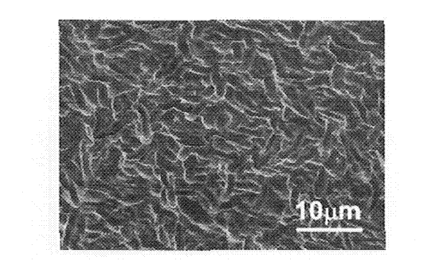
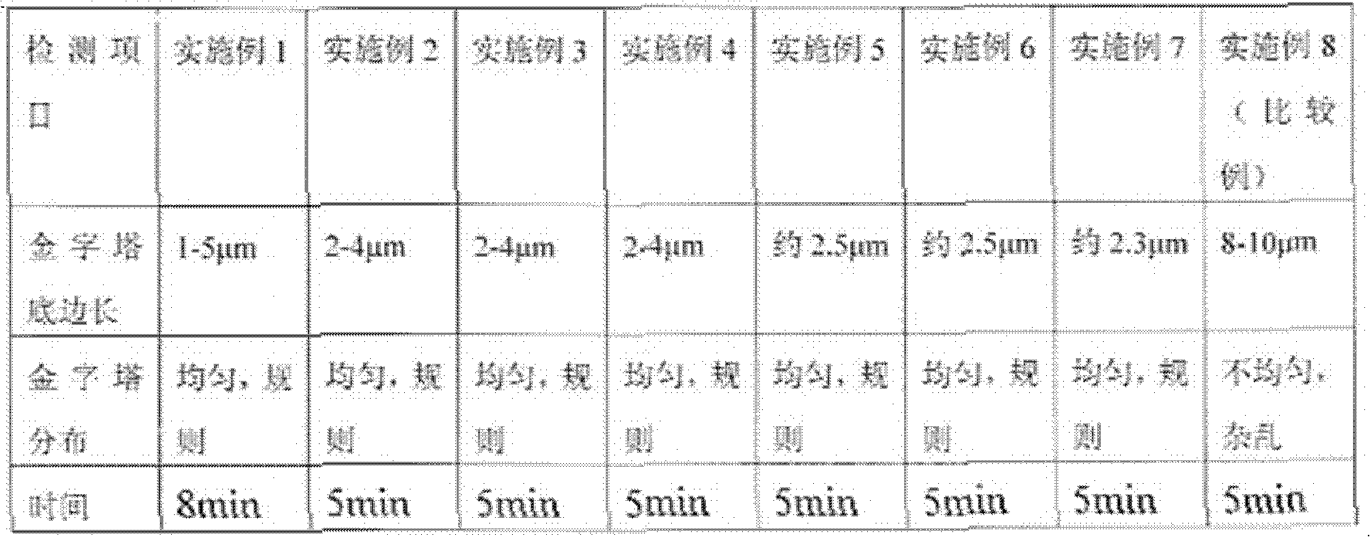
[0023] Take the following process steps: 1) configure acidic texturing solution: dissolve 5 mol / liter of sodium perchlorate and 1 mol / liter of hydrofluoric acid in deionized water; 2) immerse the polycrystalline silicon wafer for solar cells in the solution The surface is textured, the texture temperature is 7°C, and the texture time is 8 minutes.

[0024] figure 1 A scanning electron microscope plane photo of the textured surface of the obtained polycrystalline silicon wafer is given. From the figure, it can be seen that a uniform pit-shaped textured surface is formed on the surface of the silicon wafer, and the textured surface has a size of about 1-5 μm.

Embodiment 2

[0026] Take the following process steps: 1) configure acidic texturing solution: dissolve the polymethylsiloxane of 30 mol / liter of sodium perchlorate and 20 mol / liter of hydrofluoric acid, 0.05% (percentage by weight) in deionized in water; 2) immerse the polysilicon wafer for solar cells in the solution for surface texturing, the texturing temperature is 10° C., and the texturing time is 5 minutes.

Embodiment 3

[0028] Take the following process steps: 1) configure acidic cashmere liquid: the octylphenol polyoxyethylene ether of 10 mol / liter of sodium perchlorate and 5 mol / liter of hydrofluoric acid, 0.2% (percentage by weight) is dissolved in Ionized water: 2) Immerse the polysilicon wafer for solar cells into the solution for surface texturing, the texturing temperature is 10° C., and the texturing time is 5 minutes.


PUM


Abstract

The invention provides an acidic texturing solution for texturing of a polycrystalline silicon chip and a using method thereof. The acidic texturing solution is characterized in that: when the acidic texturing solution is used for surface texturing of the polycrystalline silicon chip for a solar cell, excellent texturing effect can be achieved. The technical problems of environmental pollution of the texturing solution and textured surface non-uniformity caused by instable states of the texturing solution and the process conditions in the prior art are solved.

Description

technical field [0001] The invention relates to an acidic texturing solution for texturing polycrystalline silicon wafers and its application method. Background technique [0002] In the process of preparing solar cells, in order to improve the performance and efficiency of solar cells, it is necessary to make a textured surface on the surface of the silicon wafer. The effective textured structure can make the incident sunlight reflect and refract multiple times on the surface of the silicon wafer, changing the incident light. The way forward in silicon. On the one hand, the optical path is extended, thereby increasing the absorption rate of infrared light by the silicon wafer; on the other hand, more photons are absorbed in the area near the pn junction to generate photo-generated carriers, and these photo-generated carriers are more It is easy to be collected, thus increasing the collection efficiency of photogenerated carriers. [0003] For polycrystalline silicon solar...

Claims


Application Information

Patent Timeline
Patent Type & Authority Applications(China)
IPC IPC(8): C30B33/10C23F1/24
Inventor 李明符黎明陈培良
Owner CHANGZHOU SHICHUANG ENERGY CO LTD
Why Eureka
Try Eureka