

Resistance random access change memory device
A technology of random access memory and variable resistance type, which is applied in the field of variable resistance random access memory devices, and can solve the problems of high integration difficulty, low yield, and low yield, etc.
- Summary
- Abstract
- Description
- Claims
- Application Information
AI Technical Summary
Problems solved by technology
Method used
Image

Examples
no. 1 example
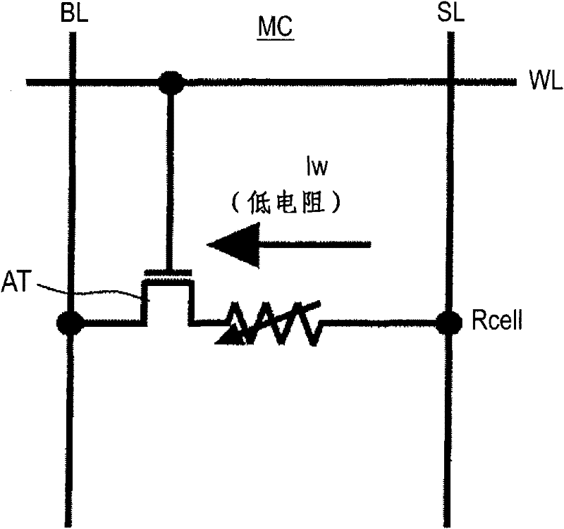
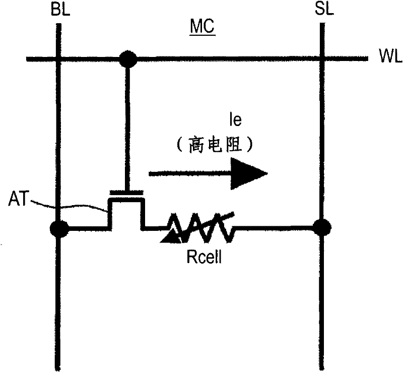
[0068] memory cell structure
[0069] Figure 1A and Figure 1B is an equivalent circuit diagram of a memory cell of an embodiment of the present invention. Notice, Figure 1A Indicates the direction of the write current Iw, Figure 1B Indicates the direction of the erase current Ie, Figure 1A and Figure 1B The memory cell structure is the same.
[0070] Figure 1A and Figure 1B The shown memory cell MC has a variable resistance element Rcell and an access transistor AT.
[0071] One end of the variable resistance element Rcell is connected to the power supply line SL, and the other end is connected to the source of the access transistor AT. The drain of access transistor AT is connected to bit line BL, and the gate is connected to word line WL.
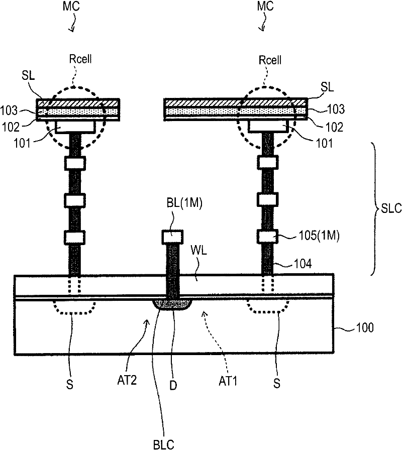
[0072] figure 2 The device structure of the corresponding parts of two adjacent memory cell parts is shown. figure 2 It is a schematic cross-sectional view without occlusion. in addition, figure 2 Vacant portions not ...
example 1
[0164] Figure 14 A modified example of the processed shape of the power supply line SL is shown.
[0165] Such as Figure 14 As shown, the processed shape of the power supply line SL may be formed to be wider in a portion of the power supply line contact portion SLC and narrower in other portions. In this processed shape, there is an advantage that the average width of the space is widened, the removability of the wiring material (removability of the etched portion) is improved, whereby the yield is made higher.
[0166] Thus, the line width of the power supply lines in the row direction can be made smaller than twice the pitch of the power supply lines in the row direction.
example 2
[0168] Figure 15 A modified example of the overlapping width of the power line contact portion SLC and the power line SL is shown.
[0169] Such as Figure 15 As shown, if the upper surface of the power supply line contact portion SLC is not completely covered by the power supply line SL, the characteristics of the memory will not be damaged. According to the structure of the variable resistance element Rcell, the variable resistance element Rcell ( Figure 15 not shown) is smaller than the size of the power line contact portion SLC.
[0170] Thus, the line width of the power supply lines in the row direction can be made smaller than twice the pitch of the power supply lines in the row direction.
[0171] Driving Circuit and Operation Example
[0172] Figure 16 Circuits showing main parts of the BL driver 10 and the SL driver 12 connected to the memory cell array 1 .
[0173] Figure 16 The shown driving circuit (10, 12) includes five NAND circuits NA...
PUM
 Abstract
Description
Claims
Application Information