Flash memory device with single-poly structure and method for manufacturing the same

A technology of flash memory device and polycrystalline structure, which is applied in semiconductor/solid-state device manufacturing, electric solid-state devices, semiconductor devices, etc., and can solve problems such as unit size reduction, large area, complex unit structure, etc.

Inactive Publication Date: 2008-03-12
DONGBU HITEK CO LTD
View PDF1 Cites 2 Cited by
  • Summary
  • Abstract
  • Description
  • Claims
  • Application Information

AI Technical Summary

Problems solved by technology

Also, since the control gates, NMOS and PMOS read transistors, channels or carrier injection regions, etc. are formed in parallel to the substrate surface, there is a limit to cell size reduct

Method used


Image

  • Flash memory device with single-poly structure and method for manufacturing the same
  • Flash memory device with single-poly structure and method for manufacturing the same
  • Flash memory device with single-poly structure and method for manufacturing the same

Examples


Example Embodiment

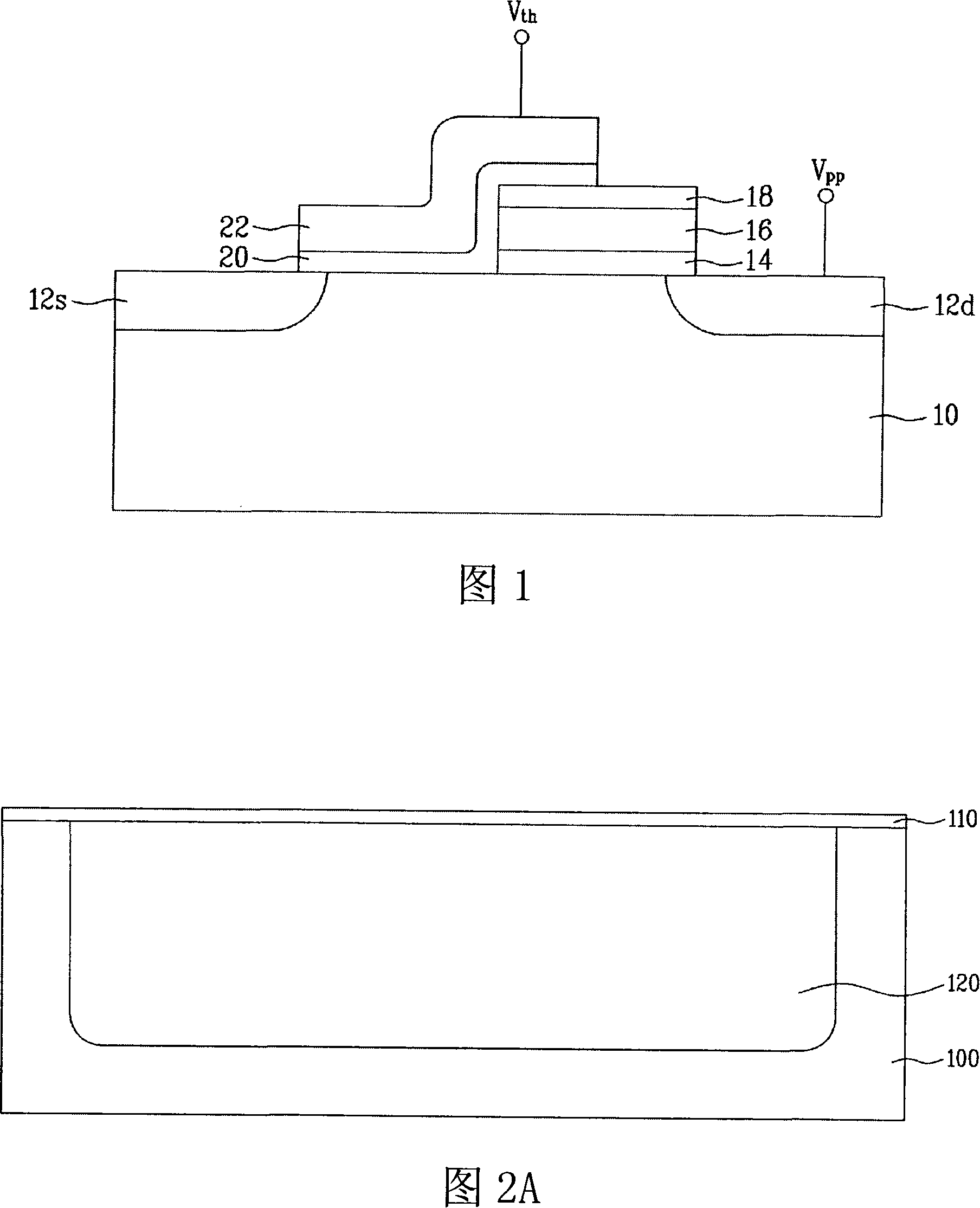
[0020] Embodiments of the present invention will now be described in detail with reference to the embodiments depicted in the accompanying drawings. Wherever possible, the same reference numbers will be used throughout the drawings to refer to the same or like parts.
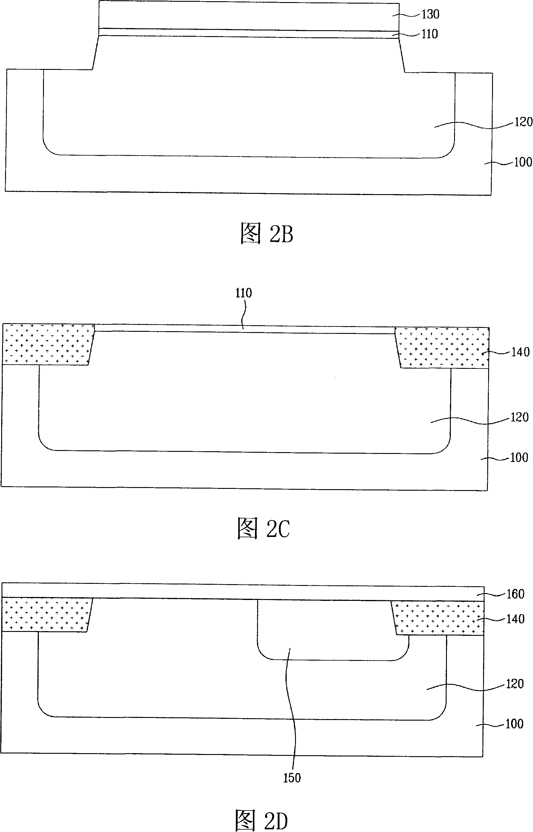
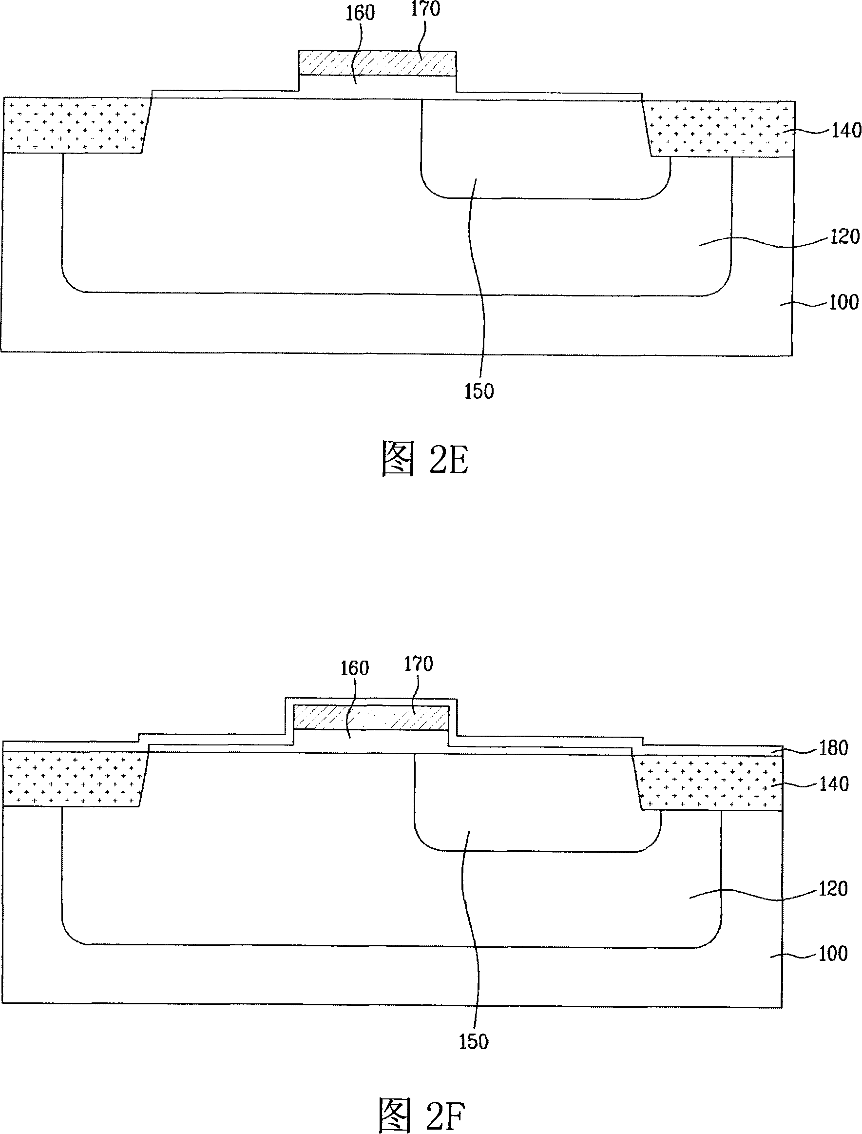
[0021] Hereinafter, a flash memory device having a single polycrystalline structure and a manufacturing method thereof according to a preferred embodiment of the present invention will be described with reference to FIGS. 2A to 2H.

[0022] First, as shown in FIG. 2A , an oxide layer 110 is formed on the semiconductor substrate 100 , and dopants are implanted into the semiconductor substrate 100 to form an HP well or HN well region 120 .

[0023] Then, in order to form shallow trench isolation (STI) as shown in FIG. 2B , photoresist 130 is disposed over regions of oxide layer 110 excluding regions used to form device insulating layers (not shown). When the oxide layer 110 is etched using the photoresist 130 as ...


PUM


Abstract

A flash memory device has a single-poly structure. A method for manufacturing the flash device includes forming an oxide layer over a semiconductor substrate having a P-well region or N-well region. A shallow trench isolation (STI) may be formed in the semiconductor substrate and the oxide layer. A drift region may be formed by injecting a dopant into a part of the P-well region or N-well region. A gate oxide layer and a poly-silicon layer may be formed over the well region, the drift region, and the STI. A control gate pattern may be formed by patterning the gate oxide layer and the poly-silicon layer. A source region and a drain region may be formed on opposite sides of the control gate pattern. A silicon nitride layer may be deposited over the control gate pattern and etching the silicon nitride layer to form a spacer around a sidewall of the control gate pattern. A plurality of insulating layers may be formed over the control gate pattern, and via-patterns may be electrically connected to the source region and the drain region, respectively. A drain electrode and a source electrode may be electrically connected to the via-patterns, respectively.

Description

[0001] This application claims the benefit of Korean Patent Application No. 10-2006-0085484 filed on Sep. 6, 2006, which application is hereby incorporated by reference. technical field [0002] The present invention relates to a semiconductor device and a manufacturing method thereof, in particular to a flash memory device with a single polycrystalline structure capable of reducing the cross-sectional area and a manufacturing method thereof. Background technique [0003] A flash memory is a programmable ROM (PROM) capable of electrically rewriting data. Flash memory is an erasable PROM (EPROM) whose storage element includes a single transistor and has a small area, but must be erased with ultraviolet light every time, and an electrically erasable PROM (EPROM) that can electrically erase data, but the storage element includes two transistors and has a large area. In addition to the combination of PROM (EEPROM). The flash memory is a device for performing a program input met...

Claims


Application Information

Patent Timeline
IPC IPC(8): H01L21/8247H01L21/336H01L27/115H01L29/78
CPCH01L27/11521H01L29/7881H01L27/11558H01L27/115H10B69/00H10B41/30H10B41/60H01L21/28141
Inventor 崔容建
Owner DONGBU HITEK CO LTD
Why Eureka
Try Eureka