

Method for manufacturing silicon-on-insulator silicon slice and floating body dynamic random access memory unit
A technology of silicon-on-insulator and manufacturing method, which is applied in the field of manufacturing silicon-on-insulator silicon wafers, and can solve problems such as performance degradation and electron leakage
- Summary
- Abstract
- Description
- Claims
- Application Information
AI Technical Summary
Problems solved by technology
Method used
Image

Examples
Embodiment Construction
[0028] In order to make the above objects, features and advantages of the present invention more clearly understood, the specific embodiments of the present invention will be described in detail below with reference to the accompanying drawings.
[0029] In the following description, numerous specific details are set forth in order to provide a thorough understanding of the present invention. However, the present invention can be implemented in many other ways different from those described herein, and those skilled in the art can make similar promotions without departing from the connotation of the present invention. Therefore, the present invention is not limited by the specific implementation disclosed below.
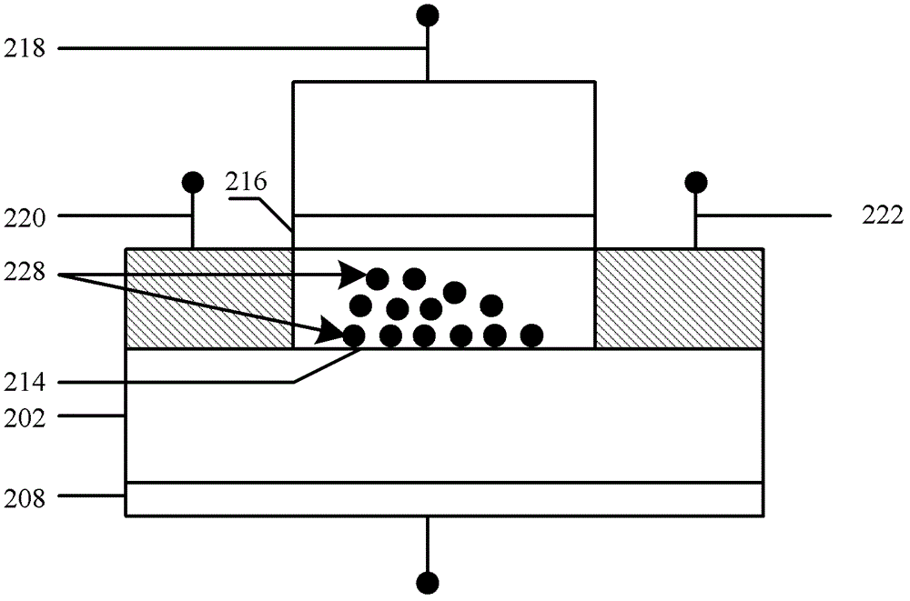
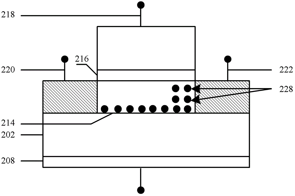
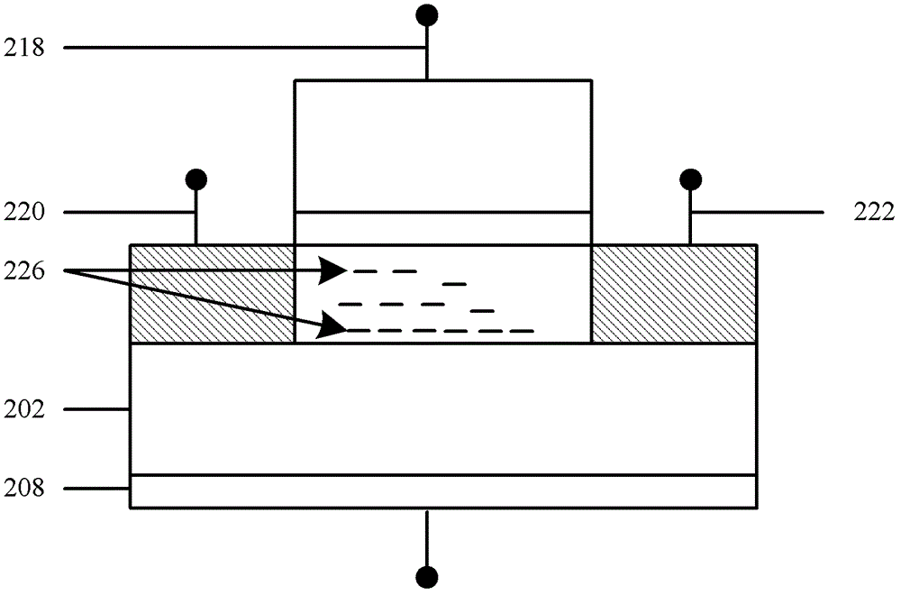
[0030]Next, the present invention is described in detail by using schematic diagrams. When describing the embodiments of the present invention in detail, for the convenience of explanation, the sectional views showing the device structure will not be partially enlarge...
PUM
 Abstract
Description
Claims
Application Information