Check patentability & draft patents in minutes with Patsnap Eureka AI!

Static random access memory (SRAM) circuit device employing hierarchical bit lines and two-stage sensitive amplifier

A technology of sensitive amplifiers and hierarchical bit lines, which is applied in the direction of instruments, static memory, digital memory information, etc., can solve the problems of increasing the reading delay and increasing the buffer level, so as to reduce the circuit access delay, increase the speed, and improve the speed effect

Active Publication Date: 2012-01-25
SHENZHEN GRADUATE SCHOOL TSINGHUA UNIV
View PDF2 Cites 17 Cited by
  • Summary
  • Abstract
  • Description
  • Claims
  • Application Information

AI Technical Summary

Problems solved by technology

For larger-capacity SRAM chips, this shortcoming becomes more prominent. The simulation results show that the global interconnection delay of large-capacity SRAM chips accounts for more than 20% of the overall access time.
Moreover, the first-stage sense amplifier needs to drive such a long global data line, and buffer stages and larger drivers must be added, which will further increase the read delay.

Method used


Image

  • Static random access memory (SRAM) circuit device employing hierarchical bit lines and two-stage sensitive amplifier
  • Static random access memory (SRAM) circuit device employing hierarchical bit lines and two-stage sensitive amplifier
  • Static random access memory (SRAM) circuit device employing hierarchical bit lines and two-stage sensitive amplifier

Examples


Embodiment Construction

[0016] The present invention will be described in more detail below in conjunction with the accompanying drawings and embodiments.

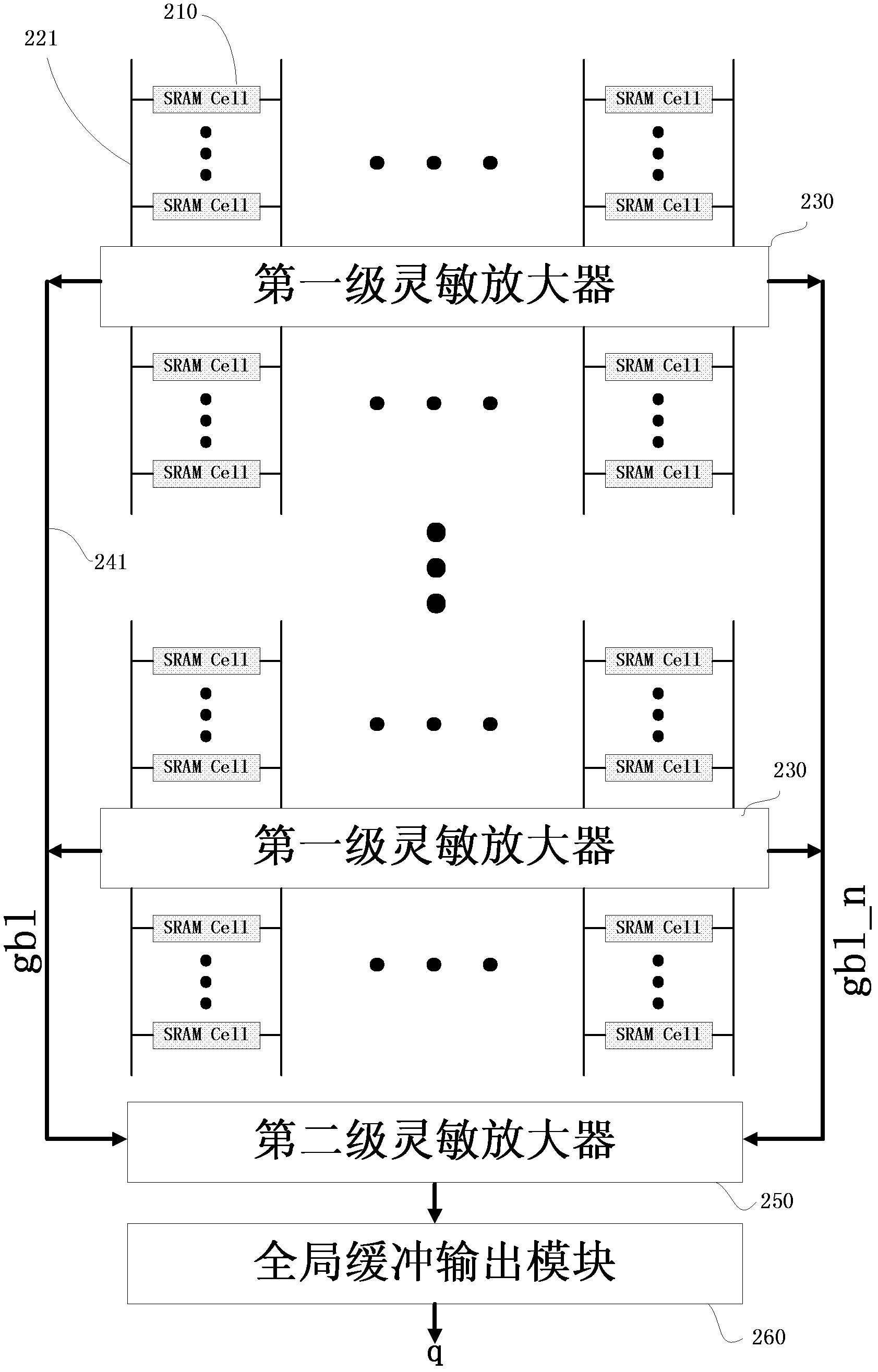
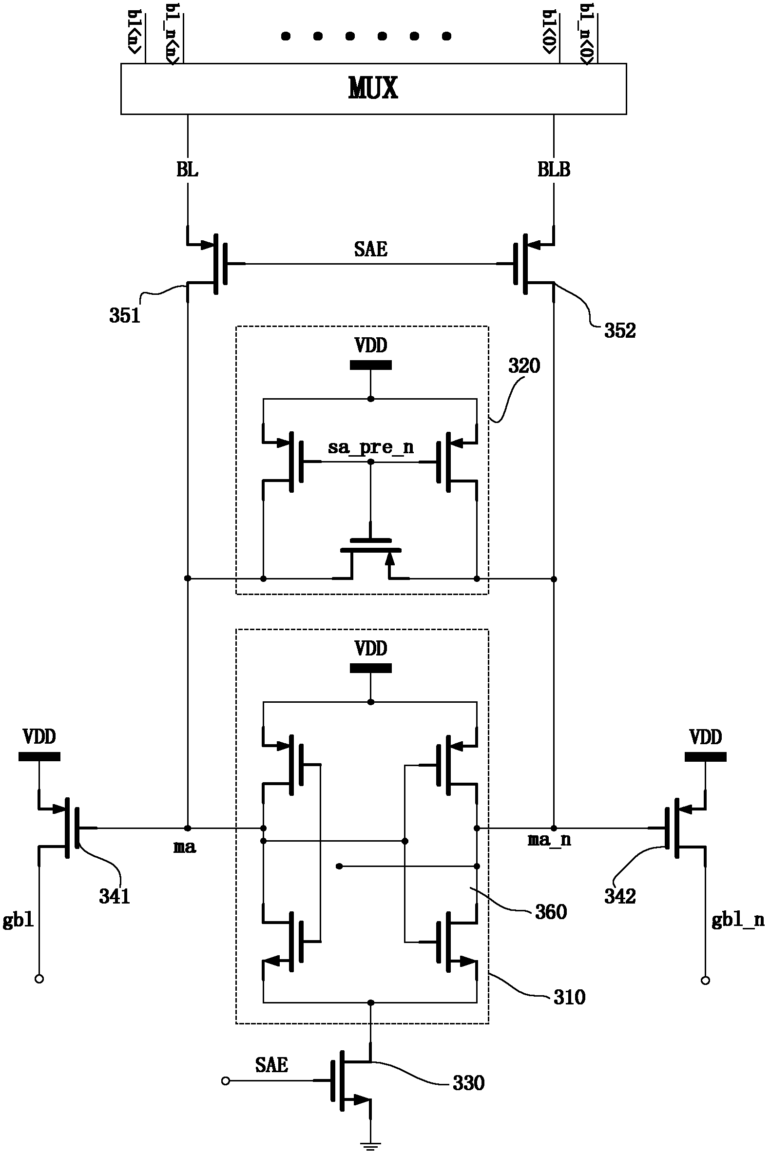
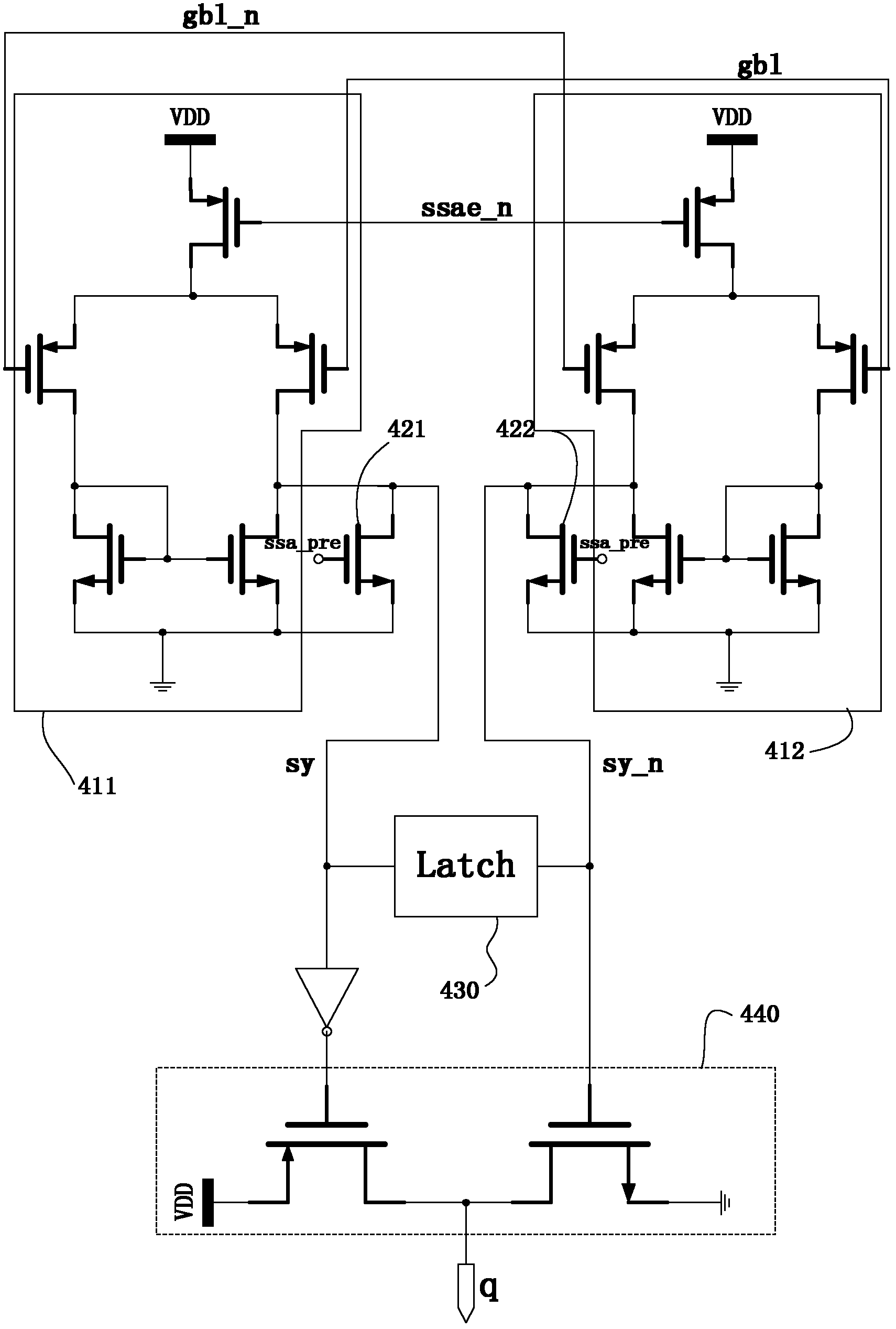
[0017] Such as figure 1 As shown, the SRAM circuit device adopting hierarchical bit lines and two-stage sense amplifiers, this embodiment includes more than one SRAM cell array, and each SRAM cell array includes sixty-four SRAM cells 210, and each SRAM cell array in each SRAM cell array Each SRAM cell 210 is connected with two local bit lines 221 corresponding to the SRAM cell array, and the two local bit lines 221 form a local bit line group, and more than one local bit line group is corresponding to a first The first-stage sense amplifiers 230 are electrically connected, and eight first-stage sense amplifiers 230 form a first-stage sense amplifier row, and the output ports of all first-stage sense amplifiers 230 of the same first-stage sense amplifier row are all the same as the corresponding two global The bit lines 241 are electrically conne...


PUM


Abstract

The invention relates to a static random access memory (SRAM) circuit device employing hierarchical bit lines and a two-stage sensitive amplifier. The circuit device is divided into subarrays; in each subarray, each local bit line is hung with a SRAM unit correspondingly by using divided bit line number; a first stage sensitive amplifier has a latch type structure; two input nodes and output nodes of inverters which are crossed and coupled are respectively driven for a global bit line through a P-channel metal oxide semiconductor (PMOS) transistor, so a signal after amplification of local bitlines is not required to be buffered and used for directly driving the global bit line. Compared with the conventional scheme, the speed can be increased. A second stage sensitive amplifier adopts a pair of complementary differential amplifiers, starts working before the first stage sensitive amplifier is opened, responses to changes of the global bit line, and amplifies differential data on the global bit line to full amplitude for output. A complementary structure is adopted in the invention and favorable for latching of the data and final driving output; compared with the traditional structure, the circuit employing the hierarchical bit lines and a two-stage amplification mechanism has the advantages that: the access delay is reduced by 15 percent, and the speed of a SRAM is effectively increased.

Description

technical field [0001] The invention belongs to the technical field of semiconductor integrated circuit devices, in particular to an SRAM circuit device using hierarchical bit lines and two-stage sensitive amplifiers. Background technique [0002] Static random access memory (SRAM) has high speed and low power consumption in semiconductor memory, and is widely used in SoC systems. Due to its fast access speed, SRAM is often used in high-speed Cache that communicates directly with the CPU. [0003] At present, for large-capacity SRAMs, the designer's design solution to increase the access speed is mainly to reduce the discharge time of the bit line in the critical path. The bit line discharge time is closely related to the capacitance of a single bit line, and the bit line capacitance is proportional to the number of mounted six-transistor units. [0004] Currently, techniques of dividing smaller sub-arrays and dividing bit lines are commonly used to reduce the load capacit...

Claims


Application Information

Patent Timeline
Patent Type & Authority Applications(China)
IPC IPC(8): G11C11/413
Inventor 刘鸣陈虹郑翔曹华敏高志强王志华
Owner SHENZHEN GRADUATE SCHOOL TSINGHUA UNIV
Features
  • R&D
  • Intellectual Property
  • Life Sciences
  • Materials
  • Tech Scout
  • Unparalleled Data Quality
  • Higher Quality Content
  • 60% Fewer Hallucinations
Learn More