High-reliability image sensor packaging structure without silicon through hole

An image sensor and packaging structure technology, applied in radiation control devices and other directions, can solve the problems of wafer-level image sensor packaging process difficulty, complex packaging structure, poor insulation in the hole, etc., to avoid poor reliability and process difficulty. The effect of reducing and simplifying the packaging process

Inactive Publication Date: 2012-02-01
JIANGYIN CHANGDIAN ADVANCED PACKAGING
View PDF9 Cites 4 Cited by
  • Summary
  • Abstract
  • Description
  • Claims
  • Application Information

AI Technical Summary

Problems solved by technology

Due to the introduction of through-silicon via interconnection in this wafer-level image sensor packaging method, the packaging structure is complicated; and the through-silicon via interconnection technology is not yet mature, often due to poor insulation in the hole, incomplete interconnection windows, and incomplete metal filling. Leading to failure or p

Method used


Image

  • High-reliability image sensor packaging structure without silicon through hole
  • High-reliability image sensor packaging structure without silicon through hole
  • High-reliability image sensor packaging structure without silicon through hole

Examples


Embodiment Construction

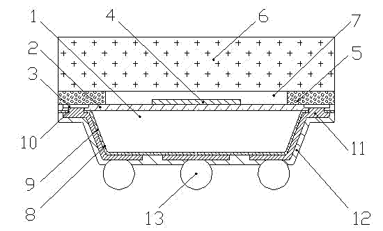
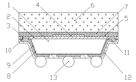
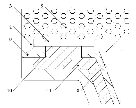
[0021] see figure 1 , figure 1 It is a cross-section schematic diagram of the packaging structure (with cavity type) of the high-reliability image sensor without through-silicon vias of the present invention. Depend on figure 1 It can be seen that the packaging structure of the high-reliability image sensor without TSVs in the present invention includes the chip body 1 provided with the passivation layer 2 inside the chip, the metal layer 3 inside the chip and the photosensitive area 4, the passivation layer inside the chip, the chip inside the chip Both the internal metal layer and the photosensitive area are structures of the image sensor chip itself, and do not belong to the packaging category involved in the patent of the present invention. An isolation layer 5 is provided on the upper surface of the chip body 1 , and the isolation layer 5 does not cover the photosensitive region 4 of the chip. A light-transmitting cover plate 6 is arranged on the isolation layer 5 . A...


PUM


Abstract

The invention relates to a high-reliability image sensor packaging structure without a silicon through-hole, comprising a chip body (1), wherein an isolated layer (5) is arranged on the upper surface of the chip body, and the isolated layer (5) is provided with a nonopaque cover plate (6); a silicon groove (8) is formed on the chip body; the lower surface of the chip body, a side wall of the silicon groove (8) and the lower surface of an exposed passivation layer (2) in the chip are selectively provided with an insulating layer (9); a blind hole (10) is formed on the exposed passivation layer (2) in the chip; a metal line layer (11) is formed on the surface of the insulating layer (9) and in the blind hole (10) selectively; a line protective layer (12) is arranged on the insulating layer (9) and the metal line layer (11) selectively; and a solder ball (13) is arranged at a position that the metal line layer (11) is exposed out of the line protective layer (12). The structure has the advantages of simple structure, good interconnection reliability, simple technology and low cost.

Description

technical field [0001] The invention relates to a packaging structure of a wafer-level image sensor. It belongs to the technical field of semiconductor packaging. Background technique [0002] An image sensor is a semiconductor device that converts external light signals into electrical signals, and the obtained electrical signals are processed for final imaging. Wafer-level image sensor packaging is a new type of image sensor packaging. Compared with traditional lead-bonded packaging, it has the advantages of small package size, low price, and the photosensitive area is not easily polluted during downstream assembly. It is being more and more popular. Much attention. Since the chip electrodes of the image sensor or the internal metal layer and the photosensitive area of ​​the chip are located on the front of the chip, wafer-level packaging needs to reserve the front of the chip as a photosensitive window, and redistribute the internal metal layer of the chip from the fron...

Claims


Application Information

Patent Timeline
IPC IPC(8): H01L27/146
Inventor 张黎陈栋赖志明陈锦辉段珍珍
Owner JIANGYIN CHANGDIAN ADVANCED PACKAGING
Why Eureka
Try Eureka