Complementary metal oxide semiconductor (CMOS)-process-based Hall switch offset voltage elimination method and circuit

An offset voltage, Hall switch technology, applied in electronic switches, electrical components, pulse technology, etc., can solve the problem of affecting the output state of the Hall switch, cannot completely eliminate the effect of the Hall chip offset voltage, and does not consider the hysteresis comparator offset voltage and other problems to achieve the effect of eliminating offset voltage

Active Publication Date: 2012-02-01
SHANGHAI ORIENT CHIP TECH CO LTD
View PDF6 Cites 22 Cited by
  • Summary
  • Abstract
  • Description
  • Claims
  • Application Information

AI Technical Summary

Problems solved by technology

This method not only does not consider the offset voltage of the hysteresis comparator, but also cannot completely eliminate the influence of the offset voltage of the Hall sheet. As the Hall voltage further decreases, the influence of the offset voltage will gradually appear, and even affect the Hall switch. output state

Method used


Image

  • Complementary metal oxide semiconductor (CMOS)-process-based Hall switch offset voltage elimination method and circuit
  • Complementary metal oxide semiconductor (CMOS)-process-based Hall switch offset voltage elimination method and circuit
  • Complementary metal oxide semiconductor (CMOS)-process-based Hall switch offset voltage elimination method and circuit

Examples


Embodiment Construction

[0020] The present invention will be further described below in conjunction with accompanying drawing:

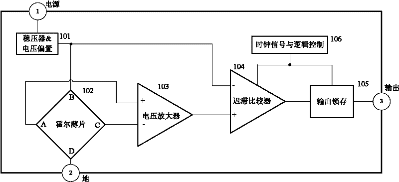
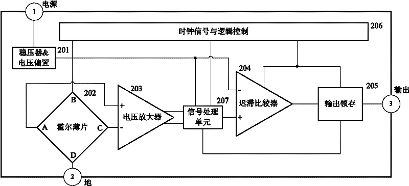
[0021] figure 2 An embodiment of the method for eliminating the offset voltage of the present invention is given, consisting of voltage regulator & voltage bias 201, Hall sheet 202, Hall voltage amplifier 203, signal processing unit 207, hysteresis comparator 204, output latch 205 and Clock signal and logic control 206 components.

[0022] The voltage regulator & voltage bias 201 provides stable voltage and current bias for other circuits, the Hall sheet 202 induces magnetic signals and converts them into voltage signals, and the voltage amplifier 203 amplifies the collected Hall voltage signals. After the signal processing unit 207, the offset voltage is eliminated, the processed voltage signal is compared with the set threshold voltage in the hysteresis comparator 204, and the corresponding voltage signal is output to the output latch 205, and the clock signal and logic...


PUM


Abstract

The invention relates to a complementary metal oxide semiconductor (CMOS)-process-based Hall switch offset voltage elimination method and a CMOS-process-based Hall switch offset voltage elimination circuit. A first clock signal and a second clock signal which are not overlapped with each other are adopted based on a rotary current method, wherein the first clock signal controls the amplification and storage of Hall voltage when a Hall slice is in a 0-degree state, and divides the second clock signal into a third clock signal and a fourth clock signal; the third clock signal controls the amplification and storage of the Hall voltage in a 90-degree state; and the fourth clock signal controls operations and comparison between the Hall voltage and threshold voltage in the 0-degree state and the 90-degree state to eliminate the offset voltage of the Hall slice. Compared with the prior art, the invention can use relatively fewer components and parts based on a CMOS process, so that a Hall switch can be applied to the detection of weak magnetic fields under the requirements of miniaturization and low power consumption.

Description

technical field [0001] The invention relates to a Hall switch circuit, in particular to a method for eliminating the offset voltage of a Hall switch based on a CMOS process and a circuit thereof. Background technique [0002] Hall effect is a kind of magnetoelectric effect. This phenomenon was discovered by American physicist Hall (A.H.Hall, 1855-1938) in 1879 when he was studying the conductive mechanism of metals. When the current passes through the conductor perpendicular to the external magnetic field, a potential difference will appear between the two end faces of the conductor perpendicular to the magnetic field and the direction of the current. This phenomenon is the Hall effect, and this potential difference is also called the Hall voltage V H . [0003] The Hall sensor based on the Hall effect has developed into a diverse family of magnetic sensor products, which are more and more widely used in various fields of industrial control. The Hall switch is one of the a...

Claims


Application Information

Patent Timeline
Patent Type & Authority Applications(China)
IPC IPC(8): H03K17/90H03K17/16
Inventor 张良罗杰罗立权刘心泽
Owner SHANGHAI ORIENT CHIP TECH CO LTD
Why Eureka
Try Eureka