Array type diamond film and method for making the same

A technology of diamond film and manufacturing method, which is applied in chemical instruments and methods, gaseous chemical plating, metal material coating technology, etc., and can solve problems such as not easy to reduce costs

Active Publication Date: 2012-02-08
KOBE STEEL LTD
View PDF10 Cites 15 Cited by
  • Summary
  • Abstract
  • Description
  • Claims
  • Application Information

AI Technical Summary

Problems solved by technology

However, a highly oriented diamond film in which one side is 20 μm or more (in the case of a square) and polygonal diamond grains (in the case of polygonal diamond grains, the above-mentioned side corresponds to the "distance between centers of gravity") adjacent to each other has not been used until now. No example of practical manufacturing has been created in the technology so far
[0025] Also, although it has been

Method used


Image

  • Array type diamond film and method for making the same
  • Array type diamond film and method for making the same
  • Array type diamond film and method for making the same

Examples


Embodiment

[0085] Hereinafter, the present invention will be described in more detail with examples, but the present invention is not limited to the following examples, and can be appropriately changed and implemented within the scope of the purpose described above and below, and these are all included in the technical scope of the present invention .

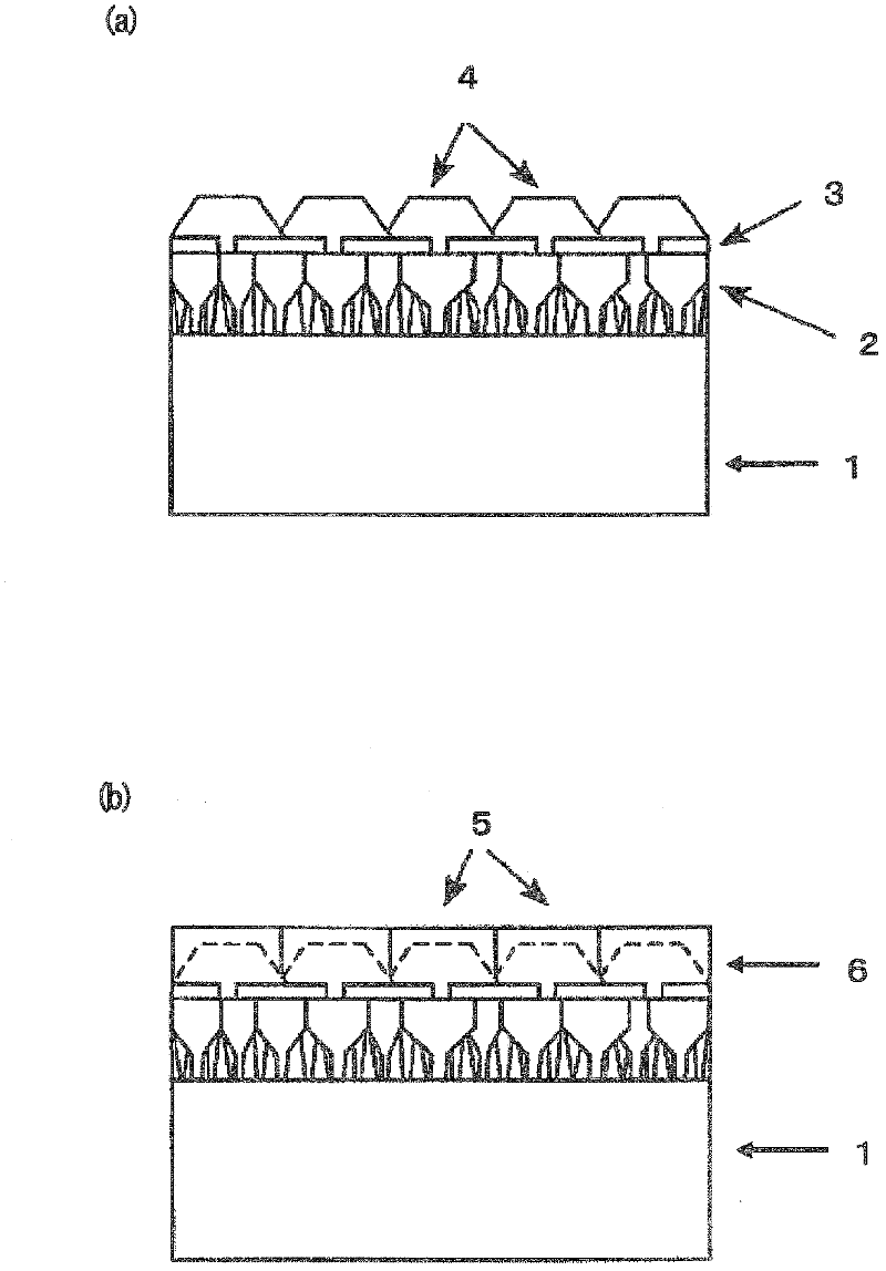
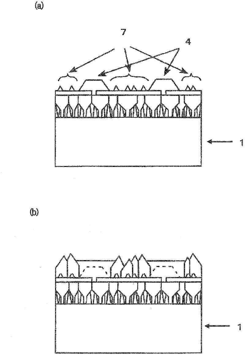
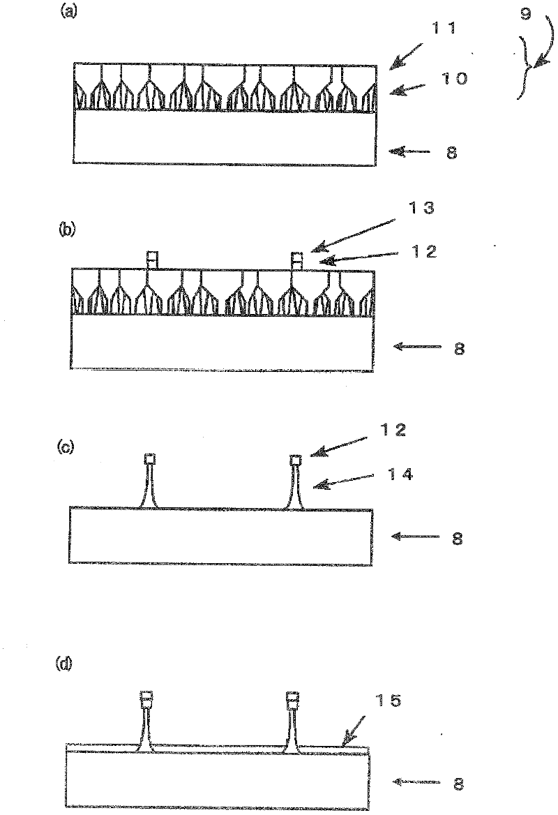
[0086] (1) Fabrication of highly oriented diamond film as the base layer

[0087] The highly oriented diamond film serving as the base layer was synthesized by the three-stage vapor phase synthesis method described in Patent Document 3. Specifically, using a Si (100) wafer as the substrate 8, surface carbonization, partial nucleus generation (first stage), orientation growth (second stage) and crystal grain Expand growth (third stage), synthesize highly oriented diamond film 9 ( image 3 (a)).

[0088] Table 1

[0089]

[0090] When the highly oriented diamond film 9 is observed by a scanning electron microscope, it is confirmed th...


PUM


Abstract

Provided is an array-type diamond film arranged with large scale polylateral diamond grains, which is configured by elements capable of easily avoiding grain boundary, thereby enable to manufacture the elements of high performance efficiently as upon a monocrystal substrate. Moreover, along the grain boundary segmentation, the element is more easily to be made. The array type diamond film, based on the information on crystallization direction, starts to grow into high orientation diamond film on the crystallized substrate of different material. On the surface, polylateral diamond grains are arranged as per the two-dimension repeating pattern with distance between the centers of gravity beyond 20 microns.

Description

technical field [0001] The present invention relates to a high-quality arrayed diamond film used in electronic devices such as transistors, diodes, light-emitting elements, and various sensors, X-ray and optical related materials, and a manufacturing method thereof. Background technique [0002] Diamond has excellent heat resistance and is usually an insulator, but it has the characteristic of being able to become a semiconductor through doping. In addition, diamond also has excellent electrical characteristics such as high dielectric surge voltage and saturation drift speed, and low permittivity. Diamond having such characteristics is expected to be used as an electronic device for high temperature, high frequency, and high electric field. [0003] In addition, due to its large band gap (5.5eV), diamond is recommended for applications such as photosensors and light-emitting elements corresponding to short-wavelength regions such as ultraviolet rays, or applications for X-r...

Claims


Application Information

Patent Timeline
IPC IPC(8): C30B29/04C30B25/00C23C16/27
Inventor 横田嘉宏橘武史
Owner KOBE STEEL LTD
Why Eureka
Try Eureka