Preparation method for semiconductor sample of TEM

A sample preparation and semiconductor technology, which is applied in the field of semiconductors, can solve the problems of easy distortion and damage of TEM samples, low success rate, difficulty in meeting the thickness requirements of TEM samples, etc., and achieve the effect of improving the success rate of preparation

Active Publication Date: 2012-02-08
SEMICON MFG INT (SHANGHAI) CORP +1
View PDF2 Cites 28 Cited by
  • Summary
  • Abstract
  • Description
  • Claims
  • Application Information

AI Technical Summary

Problems solved by technology

[0010] In view of this, the technical problem solved by the present invention is: in the TEM sample preparation of the semiconductor device located at the bottom of the wafer, due to the distance between the target structure and the sam

Method used


Image

  • Preparation method for semiconductor sample of TEM
  • Preparation method for semiconductor sample of TEM
  • Preparation method for semiconductor sample of TEM

Examples


preparation example Construction

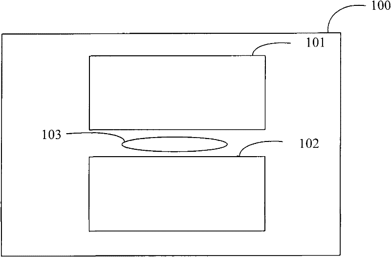
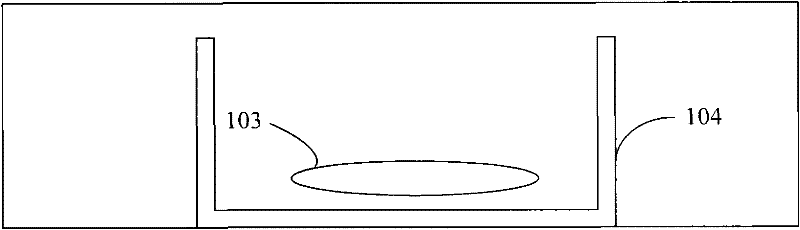
[0033] Putting the wafer into a focused ion beam machine, using a focused ion beam to form grooves on the wafer, the target structure is located between the two grooves, and the preparation method further includes:

[0034] Roughly cutting the sidewall parts of the two grooves close to the sample to obtain a sample containing the target structure;

[0035] cutting a lateral opening in the bottom of the sample to a length capable of isolating the target structure from the wafer;

[0036] Using a focused ion beam to remove semiconductor devices on the wafer above the target structure in the sample;

[0037] Finally, the focused ion beam is used to finely cut the side wall of one of the grooves close to the sample until the target structure is observed, and then finely polish the side wall of one of the grooves close to the sample until the thickness of the sample meets the requirements of the transmission electron microscope sample.

[0038] The thickness of the rough-cut sample ...

specific Embodiment 1

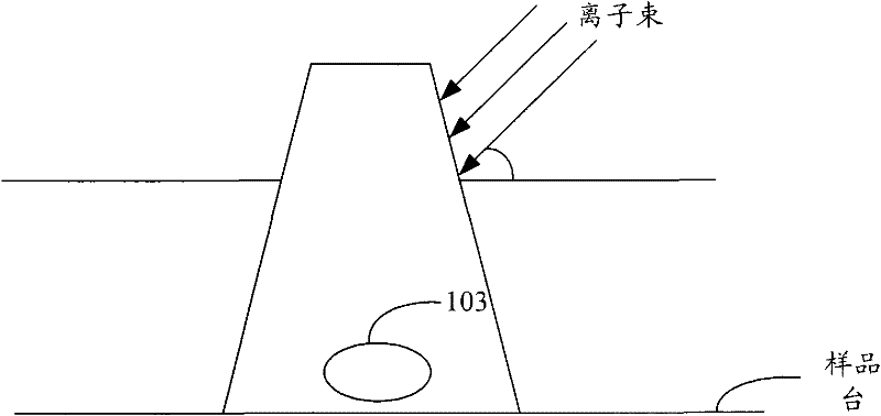
[0045] In conjunction with the TEM sample preparation flow chart of the present invention figure 2 and sample cross-sections during sample preparation image 3 In detail, the present invention uses the FIB machine with the FIB-SEM dual-beam system to carry out the TEM sample preparation method of the semiconductor device located at the bottom of the wafer, and the steps are as follows:

[0046] Step 201, place the wafer horizontally on the sample stage of the FIB machine with the FIB-SEM dual-beam system, and use a beam current range of 6000-8000 picoamps (pA) in the upper and lower symmetrical areas about 2 microns away from the target structure The I beam bombards to form a groove whose length is at least greater than the length of the target structure, the width ranges from 6 to 10 microns, and the height is at least exposing the entire target structure. The target structure is required to be located between two grooves. Among them, the position of the target structure h...


PUM

PropertyMeasurementUnit
Thickness rangeaaaaaaaaaa
Thicknessaaaaaaaaaa

Abstract

The present invention provides a preparation method for a semiconductor sample of a transmission electron microscope (TEM). The method comprises: forming a sample containing a target structure on a wafer, and cutting the sample into the sample with a thickness of about 1 micrometer through focused ion beam (FIB), cutting the bottom of the sample to obtain a lateral opening, wherein at least the length of the lateral opening is provided for completely isolating the target structure and the wafer; retaining a protective layer above the target structure, and removing a semiconductor device on anupper layer of the wafer positioned above the target structure in the sample through the FIB; carrying out fine polishing for both side wall surfaces of the sample until the thickness of the sample containing the target structure region meets the requirement of the TEM sample. The energy of the focused ion beam is lost and the distribution of the focused ion beam is nonuniform due to the distancebetween the target structure and the sample surface, such that the thickness of the TEM sample can not meet the TEM requirement and the TEM sample is distorted and destroyed. With the TEM sample preparation method provided by the present invention, the problems are avoided; the FIB bombardment point is accurately calculated; the preparation success rate of the TEM sample of the semiconductor device positioned on the bottom layer of the wafer is improved.

Description

technical field [0001] The invention relates to the technical field of semiconductors, in particular to a semiconductor sample preparation method for a transmission electron microscope. Background technique [0002] Currently, transmission electron microscopy (TEM) is increasingly used for failure analysis of semiconductor devices by observing their morphology. Since the principle of TEM is that electron diffraction penetrates the sample to form an image, the requirements for sample preparation in the TEM method are very high, and the thickness of the sample is usually required to be no more than 0.1 microns. The semiconductor device structure grown on the wafer is arranged in layers. When a certain semiconductor device on the bottom layer of the wafer is used as the target structure of TEM, it is necessary to prepare a sample containing the target structure and meeting the thickness requirements of the TEM sample. . In the prior art, the focused ion beam (FIB) machine can...

Claims


Application Information

Patent Timeline
IPC IPC(8): G01N1/32
Inventor 芮志贤李剑于会生段淑卿
Owner SEMICON MFG INT (SHANGHAI) CORP
Why Eureka
Try Eureka