Solar battery assembly of copper-indium-gallium-selenium thin film and preparation method of light absorption layer thereof

A solar cell and light absorbing layer technology, applied in the field of solar cells, can solve the problems affecting the electrical properties of copper indium gallium selenium thin film solar cells, the inability to accurately realize the energy band structure, and the lack of precise control of the ratio, etc., to achieve excellent electrical properties, The effect of stable quality and high light absorption rate

Active Publication Date: 2012-02-15
THE CHINESE UNIVERSITY OF HONG KONG +1
View PDF2 Cites 13 Cited by
  • Summary
  • Abstract
  • Description
  • Claims
  • Application Information

AI Technical Summary

Problems solved by technology

The process control of this three-step co-evaporation method is relatively complicated, and the ratio between the substances is not precisely controlled during the evaporation process. This preparation method cannot accurately realize the theoretically designed energy band structure, thereby affecting the copper indium gallium selenium thin film. Electrical Properties of Solar Cells

Method used


Image

  • Solar battery assembly of copper-indium-gallium-selenium thin film and preparation method of light absorption layer thereof
  • Solar battery assembly of copper-indium-gallium-selenium thin film and preparation method of light absorption layer thereof
  • Solar battery assembly of copper-indium-gallium-selenium thin film and preparation method of light absorption layer thereof

Examples


Embodiment 1

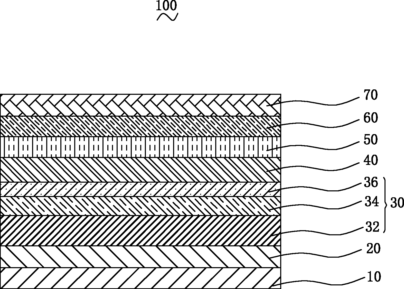
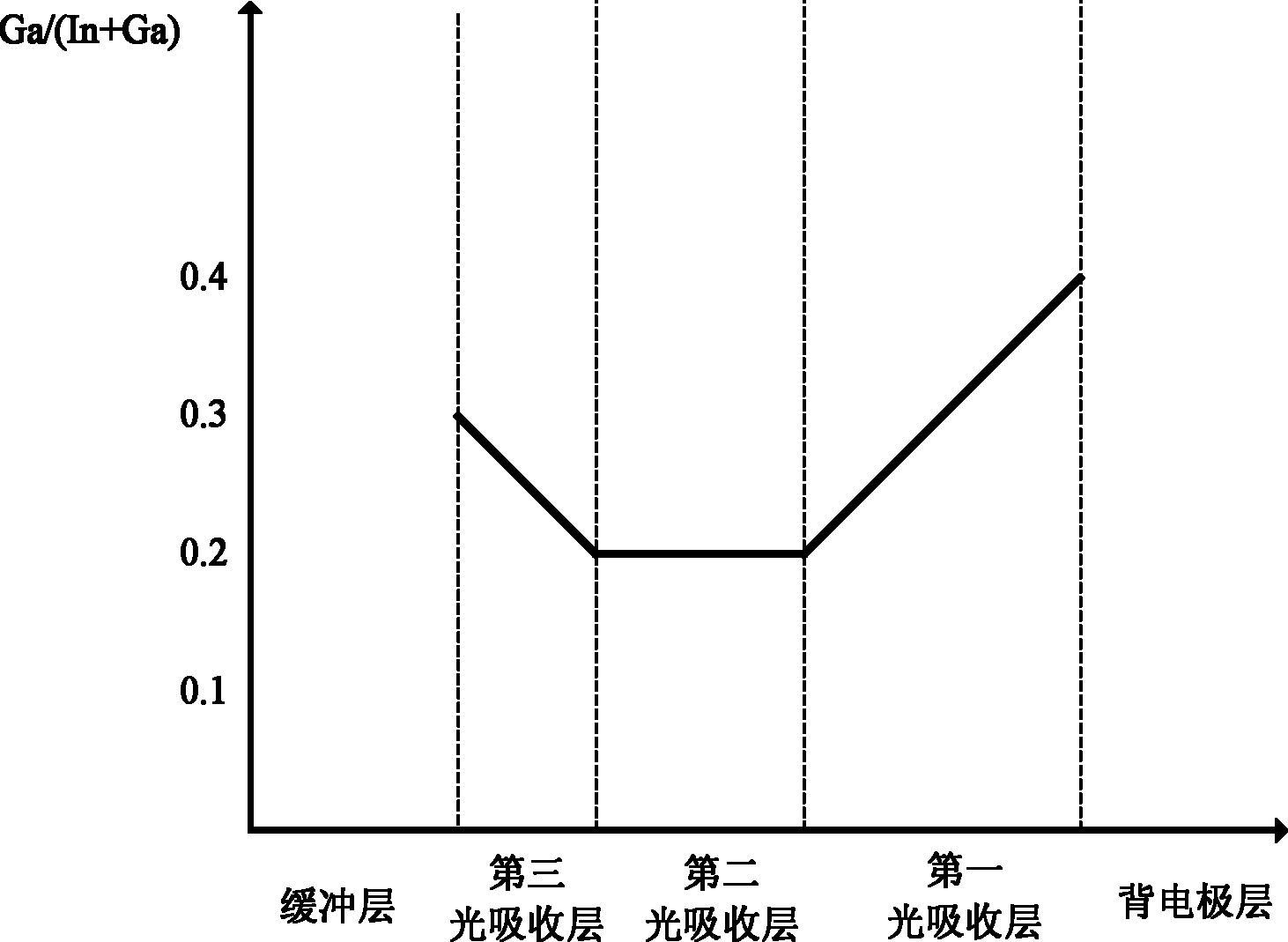
[0095] (1) Preparation of light absorbing layer 30

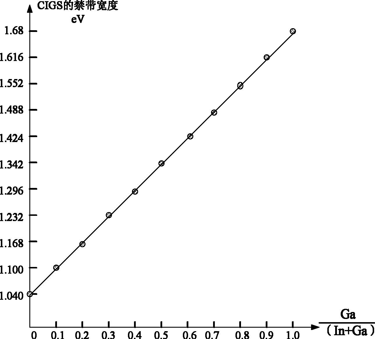
[0096] The temperature of the substrate 10 is maintained at 450° C., and then the four substances of CIGS are evaporated simultaneously at different temperatures. During the evaporation process, the evaporation temperature of selenium is always kept at 200°C, and the evaporation temperature of copper is always kept at 1300°C. During the evaporation process, the ratio of the evaporation amount of copper to the sum of the evaporation amounts of indium and gallium was 0.8.

[0097] The evaporation process consists of three stages:

[0098] The first stage: within 10 minutes, the evaporation temperature of indium is gradually and uniformly increased by 20°C from 800°C, and the evaporation temperature of gallium is gradually and uniformly decreased by 20°C from 900°C to form the first light absorbing layer 32 . The thickness of the first light absorbing layer 32 is 1000 nanometers.

[0099] Second stage: after the first stage...

Embodiment 2

[0105] (1) Preparation of light absorbing layer 30

[0106]The temperature of the substrate 10 is maintained at 600° C., and then the four substances of CIGS are evaporated simultaneously at different temperatures. During the evaporation process, the evaporation temperature of selenium is always kept at 300°C, and the evaporation temperature of copper is always kept at 1500°C. During the evaporation process, the ratio of the evaporated amount of copper to the sum of the evaporated amounts of indium and gallium was 0.95.

[0107] The evaporation process consists of three stages:

[0108] The first stage: within 8 minutes, the evaporation temperature of indium is gradually and uniformly increased by 30°C from 1000°C, and the evaporation temperature of gallium is gradually and uniformly decreased by 30°C from 1100°C to form the first light absorbing layer 32 . The thickness of the first light absorbing layer 32 is 1500 nm.

[0109] Second stage: after the first stage, keep th...

Embodiment 3

[0115] (1) Preparation of light absorbing layer 30

[0116] The temperature of the substrate 10 is maintained at 450° C., and then the four substances of CIGS are evaporated simultaneously at different temperatures. During the evaporation process, the evaporation temperature of selenium is kept at 200°C, the evaporation temperature of copper is kept at 1300°C, and the evaporation temperature of indium is kept at 800°C. During the evaporation process, the ratio of the evaporation amount of copper to the sum of the evaporation amounts of indium and gallium was 0.8.

[0117] The evaporation process consists of three stages:

[0118] First stage: within 10 minutes, the evaporation temperature of gallium is gradually and uniformly lowered from 800° C. to 30° C. to form the first light absorbing layer 32 . The thickness of the first light absorbing layer 32 is 1000 nanometers.

[0119] The second stage: after the first stage, keep the evaporation temperature of gallium at 770° C....


PUM


Abstract

The invention relates to a solar battery assembly of a copper-indium-gallium-selenium thin film, which comprises a substrate, a back electrode layer, a light absorption layer, a buffer layer, a window layer, a transparent electrode layer and a metal grid electrode layer which are overlapped in sequence, wherein a forbidden bandwidth of the light absorption layer is distributed in a trapezoid shape which is flat at the middle part and gradually-heightened at both sides in a thickness direction. With the adoption of the trapezoid structure of the forbidden band, sunlight can be absorbed within a wider spectral region to ensure the sunlight to be sufficiently absorbed by the light absorption layer, so that the light absorption rate can be improved; and meanwhile, a potential difference whichis changed to both sides of the light absorption layer is generated through the trapezoid structure of the forbidden band, and therefore the solar battery assembly of the copper-indium-gallium-selenium thin film has the advantages of higher light absorption rate and good electric properties by ensuring a short-circuit current and effectively improving an open-circuit voltage. In addition, the invention provides two preparation methods of the light absorption layer of the copper-indium-gallium-selenium thin film solar battery assembly.

Description

【Technical field】 [0001] The invention relates to solar cell technology, in particular to a copper indium gallium selenium thin film solar cell component and a preparation method for a light absorbing layer thereof. 【Background technique】 [0002] Studies have found that when the bandgap width of the CIGS light-absorbing layer of CIGS thin-film solar cells has a V-shaped distribution, it can effectively improve the electrical properties of photovoltaic cells. Compared with flat energy band distribution or unidirectional energy In the case of band distribution, the copper indium gallium selenide semiconductor thin film with V-shaped double gradient structure can increase the open circuit voltage while ensuring better current collection efficiency. However, solar cells with a V-shaped distribution of energy band structure have a wide distribution of energy bands in the light-absorbing layer, which leads to a non-steep absorption edge in the long-wave band, and insufficient abs...

Claims


Application Information

Patent Timeline
Patent Type & Authority Applications(China)
IPC IPC(8): H01L31/0352H01L31/032H01L31/18
CPCY02P70/50
Inventor 肖旭东杨春雷刘壮
Owner THE CHINESE UNIVERSITY OF HONG KONG
Why Eureka
Try Eureka