Vertical double-diffusion metal oxide semiconductor field effect transistor (MOSFET)

An oxide semiconductor, vertical double diffusion technology, applied in semiconductor devices, electrical components, circuits, etc., can solve the problems of high withstand voltage level, difficult to obtain, and limited application

Inactive Publication Date: 2012-02-29
UNIV OF ELECTRONIC SCI & TECH OF CHINA +1
View PDF4 Cites 18 Cited by
  • Summary
  • Abstract
  • Description
  • Claims
  • Application Information

AI Technical Summary

Problems solved by technology

However, as a normally-off device, the buried channel MOSFET only uses the self-depletion of the pn junction to maintain the blocking of the channel, so the leakag

Method used


Image

  • Vertical double-diffusion metal oxide semiconductor field effect transistor (MOSFET)
  • Vertical double-diffusion metal oxide semiconductor field effect transistor (MOSFET)
  • Vertical double-diffusion metal oxide semiconductor field effect transistor (MOSFET)

Examples


Embodiment Construction

[0018] The present invention is described in detail below in conjunction with accompanying drawing and embodiment:

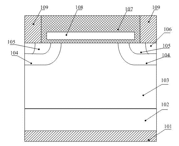
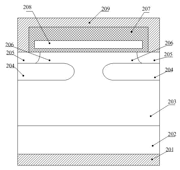
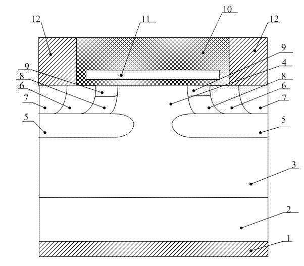
[0019] The technical scheme of the present invention is as follows, and its basic structure is as follows: image 3 shown, including metallized drain 1, N + Substrate 2, N - Drift region 3, junction field effect transistor region 4, deep P body region 5, N-type heavily doped source region 6, P-type heavily doped region 7, N-type buried layer channel 8, P-type epitaxial layer 9, gate An oxide layer 10, a polysilicon gate electrode 11, and a metallized source electrode 12. The metallized drain 1 is located on the N + Substrate 2 back side, N - Drift zone 3 is located at N + The front side of the substrate 2; the deep P body region 5 is located on the N - The two sides above the drift region 3 are connected to the N-type heavily doped source region 6 through the P-type heavily doped region 7 and the metallized source 12 to suppress the parasitic triode effect...


PUM

PropertyMeasurementUnit
Thicknessaaaaaaaaaa
Thicknessaaaaaaaaaa

Abstract

The invention discloses a vertical double-diffusion metal oxide semiconductor field effect transistor (MOSFET), which comprises a metallization drain 1, an N<+> substrate 2, an N<-> drift region 3, a deep P body region 5, an N type heavy doping source region 6, a P type heavy doping region 7, an N type buried layer channel 8, a P type epitaxial layer 9, a gate oxidation layer 10, a polysilicon gate electrode 11 and a metallization source 12. When the vertical double-diffusion MOSFET is switched on, the switch-on resistance of a device is greatly reduced through the common electricity conducting mechanism of two channels; and when the vertical double-diffusion MOSFET is switched off, electric fields of the channels are shielded through a P+N junction barrier, so that a higher voltage-resisting level of more than 1,000V is realized.

Description

technical field [0001] The invention relates to the technical field of semiconductor devices, in particular to a vertical double-diffused metal oxide semiconductor field effect transistor. Background technique [0002] In recent years, with the rapid development of microelectronics technology and the urgent needs of automotive electronics, aerospace, industrial control, power transportation and other related fields, the development of new high-power semiconductor devices has attracted more and more attention. Power MOSFET (Metal Oxide Semiconductor Field Effect Transistor) is a new generation of power electronic devices developed on the basis of MOS integrated circuit technology. And VDMOS (Vertical Double Diffused Metal Oxide Semiconductor Field Effect Transistor, see figure 1 ) has the advantages of large input impedance, fast switching speed, high operating frequency, and good thermal stability. It has been widely used in switching regulated power supplies and power ampl...

Claims


Application Information

Patent Timeline
IPC IPC(8): H01L29/10H01L29/78
Inventor 张有润张波高云斌刘影
Owner UNIV OF ELECTRONIC SCI & TECH OF CHINA
Why Eureka
Try Eureka