Manufacturing method of N-type radio frequency lateral double-diffused metal-oxide semiconductor (LDMOS)

A manufacturing method, N-type technology, applied in semiconductor/solid-state device manufacturing, electrical components, circuits, etc., can solve problems affecting device breakdown characteristics, breakdown voltage drop, etc., to improve breakdown characteristics, increase process costs, Adjustable and adaptable effects

Active Publication Date: 2012-03-14
SHANGHAI HUAHONG GRACE SEMICON MFG CORP
View PDF3 Cites 8 Cited by
  • Summary
  • Abstract
  • Description
  • Claims
  • Application Information

AI Technical Summary

Problems solved by technology

A shortcoming of the existing radio frequency LDMOS formed by the manufacturing method of the existing radio frequency LDMOS is that the interface of each layer of the multi-layer P-type epitaxial layer also includes a P-type buried layer formed by self-doping
The P-type buried layer formed by the self-doping will seriously affect the breakdown characteristics of the device, resulting in a decrease in the breakdown voltage

Method used


Image

  • Manufacturing method of N-type radio frequency lateral double-diffused metal-oxide semiconductor (LDMOS)
  • Manufacturing method of N-type radio frequency lateral double-diffused metal-oxide semiconductor (LDMOS)
  • Manufacturing method of N-type radio frequency lateral double-diffused metal-oxide semiconductor (LDMOS)

Examples


Embodiment Construction

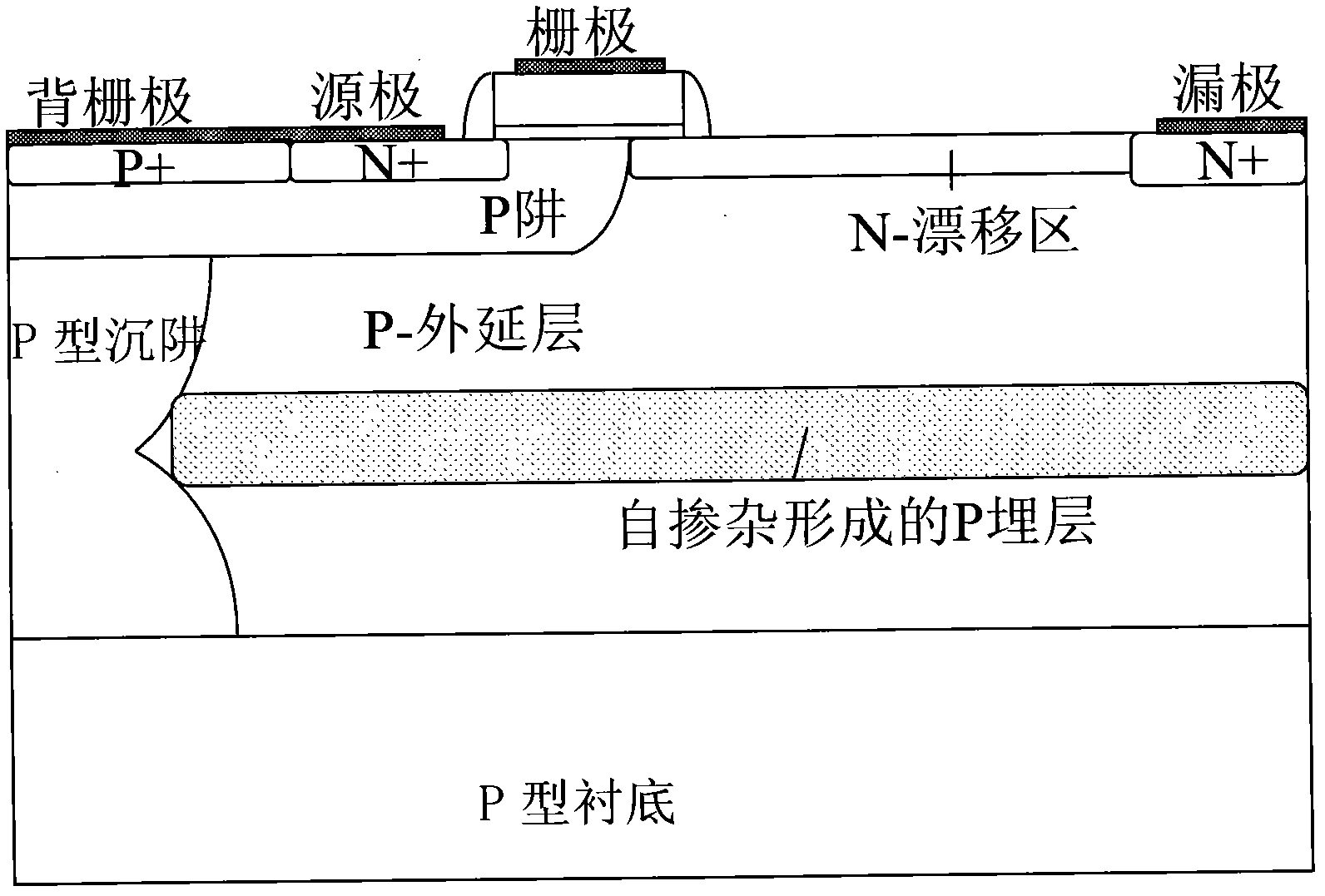
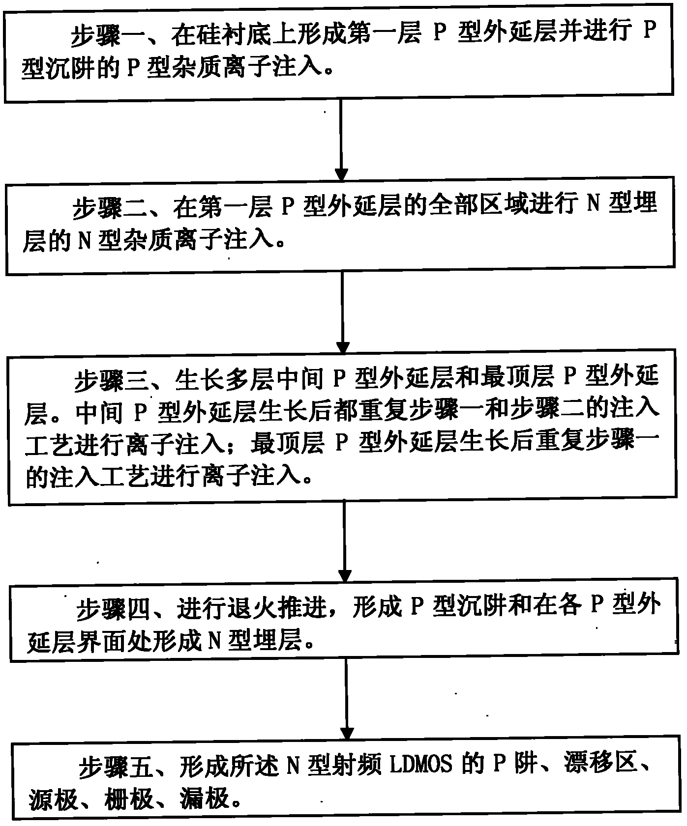
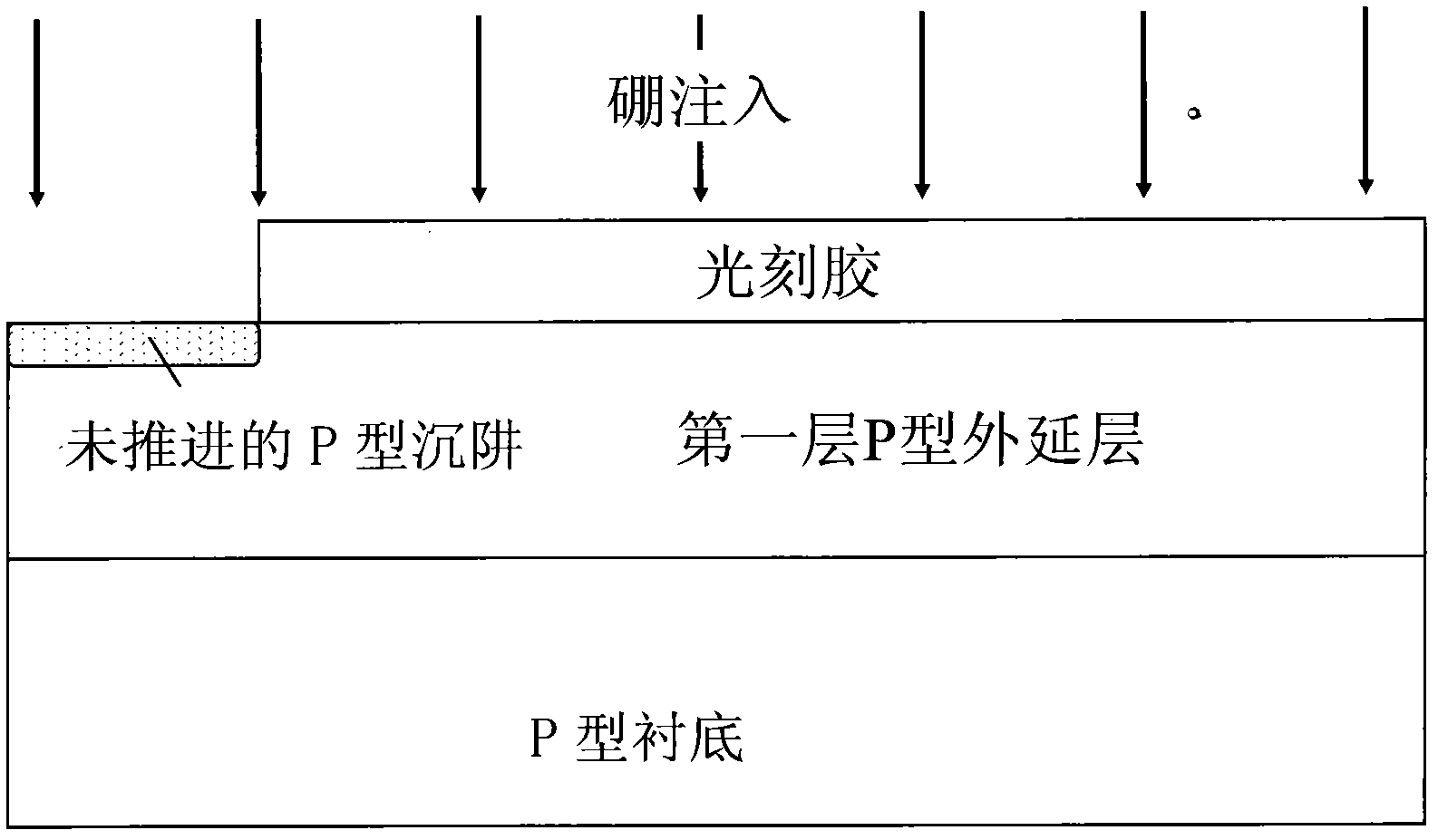
[0017] Such as figure 2 Shown, is the flow chart of the manufacturing method of radio frequency LDMOS of the present invention; As Figure 3 ~ Figure 7 As shown, it is a device schematic diagram of each step in the manufacturing method of a radio frequency LDMOS according to the embodiment of the present invention. The manufacturing method of the radio frequency LDMOS of the embodiment of the present invention comprises the following steps:

[0018] Step 1, such as image 3 As shown, the first layer of P-type epitaxial layer is formed on a heavily doped P-type silicon substrate, and the P-type sinking well is formed in the region of the first layer of P-type epitaxial layer. Type impurity ion implantation forms a non-propelled P-type sink well. The doping impurity of the first P-type epitaxial layer is boron, and the impurity body concentration is 1.0E14cm -3 ~1.0E15cm -3 . The region of the P-type sink well is defined by photoresist. The process conditions of the P-ty...


PUM


Abstract

The invention discloses a manufacturing method of an N-type radio frequency lateral double-diffused metal-oxide semiconductor (LDMOS), which comprises the steps that: a first P-type epitaxial layer is formed on a silicon substrate and the P-type impurity ion implantation of a P-type sink trap is carried out; the N-type impurity ion implantation of an N-type embedded layer is carried out in all areas of the first P-type epitaxial layer; a plurality of middle P-type epitaxial layers and a top P-type epitaxial layer are grown; the implantation processes in Steps 1 and 2 are repeated after the middle P-type epitaxial layers are grown for ion implantation; the implantation process in Step 1 is repeated after the top P-type epitaxial layer is grown for ion implantation; and annealing advance iscarried out to form the P-type sink trap and the N-type embedded layer is formed at the interfaces of the P-type epitaxial layers. The P trap of the N-type radio frequency LDMOS, a drift area, a source, a grid and a drain are formed. The method can significantly improve the breakdown characteristic of a device, is not restricted by the increased thicknesses of the epitaxial layers, and has the characteristics of low process cost, adjustability and strong applicability.

Description

technical field [0001] The invention relates to a manufacturing process method of a semiconductor integrated circuit, in particular to a manufacturing method of an N-type radio frequency LDMOS. Background technique [0002] In the existing RF LDMOS process, in order to reduce the wiring inductance and resistance of the source, improve the RF gain of the common source amplifier, reduce the unfavorable parasitic parameters caused by the source wiring and further reduce the layout area, a heavily doped sink is often used. The well connects the source to the grounded substrate to improve device performance. For applications with high withstand voltage requirements and large epitaxial layer thickness, sinker wells are usually formed by implanting sinker wells while forming the epitaxial layer, and advancing after the growth of the epitaxial layer is completed. However, due to the high concentration of sinker impurities, When the epitaxial layer grows, more sinker impurities will...

Claims


Application Information

Patent Timeline
Patent Type & Authority Applications(China)
IPC IPC(8): H01L21/335H01L21/265
Inventor 钱文生韩峰王海军
Owner SHANGHAI HUAHONG GRACE SEMICON MFG CORP
Why Eureka
Try Eureka