Manufacturing method of light-emitting device

A manufacturing method and technology for light-emitting devices, which are applied to electrical components, circuits, semiconductor devices, etc., can solve problems such as thickening, color temperature difference of white light-emitting diode products, and material shortage, reduce thickness, and improve the thickness and uniformity of phosphor powder. Problems, effects of improving stability

Inactive Publication Date: 2012-03-14
FORMOSA EPITAXY INCORPORATION
View PDF7 Cites 9 Cited by
  • Summary
  • Abstract
  • Description
  • Claims
  • Application Information

AI Technical Summary

Problems solved by technology

[0004] However, in terms of packaging technology for white light emitting diodes, when developing high-power and large-area LED lighting modules, the heat dissipation problem will seriously affect the life of the components. The method, because the packaging of light-emitting diodes used in today's industry is based on economic considerations, it is believed that epoxy resin is used for packaging, so it is easy to thicken during use, which makes it difficult to control the generation of bubbles, lack of material, and black spots in the phosphor layer. And the unavoidable defects such as phosphor powder precipitation in the fluorescent glue, and the phosphor layer is an uneven surface, so the uniformity of the color light cannot be kept consistent, and it is easy to cause the color temperature difference of white light emitting diode products at different light angles
Although white light emitting diodes have improved light extraction efficiency and light conversion efficiency with the continuous improvement of phosphor powder or encapsulant, but white light light emitting diodes also face other problems, such as: the thickness of the phosphor layer is constantly increasing, or Phosphor powder or encapsulant covers the external electrodes of white light emitting diodes, causing problems such as poor electrical contact of white light emitting diodes, and the phosphor layer is still uneven after continuous improvement, so the problem of color temperature uniformity still exists

Method used


Image

  • Manufacturing method of light-emitting device
  • Manufacturing method of light-emitting device
  • Manufacturing method of light-emitting device

Examples


Embodiment Construction

[0088] In order to have a further understanding and understanding of the structural features of the present invention and the achieved effects, the preferred embodiments and accompanying drawings are used for a detailed description, as follows:

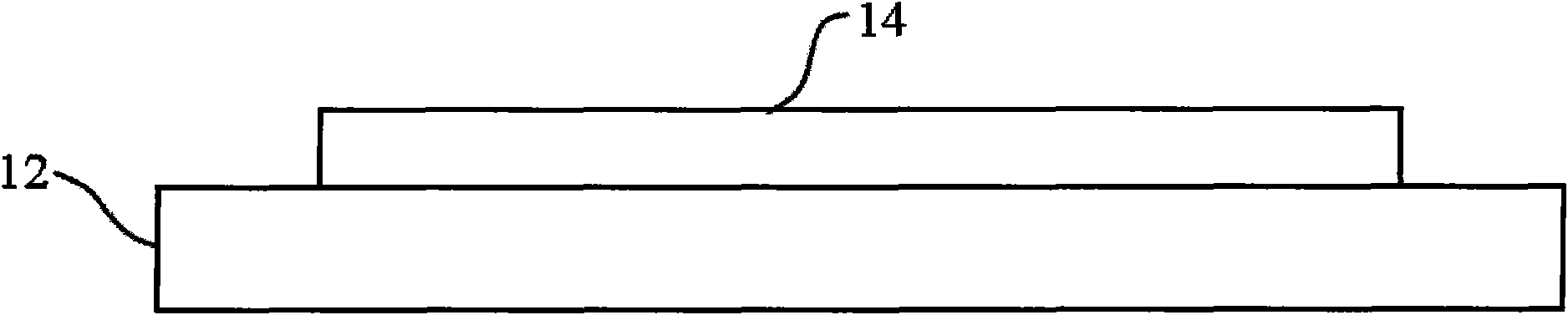
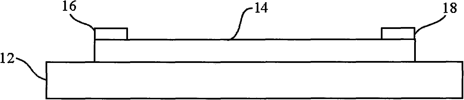
[0089] see Figure 1A to Figure 1G , which is a schematic diagram of the implementation steps of a preferred embodiment of the present invention. Such as Figure 1A to Figure 1G As shown, it represents the manufacturing process of a first light-emitting device 10 of the present invention. first as Figure 1A As shown, a substrate 12 is provided, and the material of the substrate 12 is selected from Al 2 o 3 , SiC, GaAs, GaN, AlN, GaP, Si, ZnO and MnO, III-V group, II-VI group, IV group, IV-IV group and any combination thereof. Such as Figure 1B As shown, a light-emitting unit 14 is formed on the substrate 12, wherein the light-emitting unit 14 of this embodiment is a front-side light-emitting diode chip, so as Figure 1C As sho...


PUM

PropertyMeasurementUnit
thicknessaaaaaaaaaa
wavelengthaaaaaaaaaa

Abstract

The invention relates to a manufacturing method of a light-emitting device, comprises the following steps of: firstly, providing a substrate, then forming an light-emitting unit on the substrate, forming at least one electrode, and forming at least one protective layer on the electrode, thereby preventing a fluorescent powder layer from covering the electrode when the fluorescent powder layer is formed on the light-emitting unit; and after forming the fluorescent powder layer, leveling the fluorescent powder layer and the protective layer, i.e. removing part of the fluorescent powder layer from the protective layer, then removing the protective layer, thereby preventing the electrode from being influenced by the fluorescent powder layer, and further improving the electric conductivity of the electrode, improving the thickness and uniformity of fluorescent powder of the light-emitting device, effectively reducing the thickness of the light-emitting device with a light-emitting diode, and greatly improving the stability in white light color temperature control.

Description

technical field [0001] The invention relates to a manufacturing method of a light emitting device. Background technique [0002] The world's earliest light-emitting diode products appeared in 1968 AD, and then the optoelectronic industry successively developed many color light-emitting diodes. It was not until 1993 that Japan's Nichia Company successfully developed blue-green light-emitting diodes with high luminous efficiency that the world's Colored light-emitting diode products can be realized. Because, after the development of GaInN-based blue and green light-emitting diodes is completed, white light-emitting diodes have become the object pursued by the industry. Since Nichia mass-produced white light-emitting diodes in 1996, the global light-emitting diode industry has shifted the focus of research and development to white light-emitting diodes, which can completely replace existing incandescent lamps for indoor and outdoor lighting, and will also extensively and revol...

Claims


Application Information

Patent Timeline
Patent Type & Authority Applications(China)
IPC IPC(8): H01L33/48H01L33/50
Inventor 郑惟纲林裕智廖汉忠丁逸圣潘锡明
Owner FORMOSA EPITAXY INCORPORATION
Why Eureka
Try Eureka