Electromigration test structure of silicon through hole metal interconnection wire

A test structure and through-silicon via technology, which is applied in the field of electromigration reliability test structure of through-silicon via metal interconnection, can solve the problem of directly pointing at both ends of the through-hole four-probe method, and achieve low test cost, Convenient operation and high test efficiency

Inactive Publication Date: 2012-03-21
HUAZHONG UNIV OF SCI & TECH
View PDF4 Cites 3 Cited by
  • Summary
  • Abstract
  • Description
  • Claims
  • Application Information

AI Technical Summary

Problems solved by technology

However, there are very few electromigration studies on TSV interconnection technology. In view of the different environment between electromigration of TSV interconnection technology and traditional interconnection metal wires, for example, ordinary interconnection metal wires are mostly wrapped by packaging plastics, while TSV The metal interconnection in the hole of the through-silicon via is wrapped by the silicon substrate, so it is necessary to test the electromigrat

Method used


Image

  • Electromigration test structure of silicon through hole metal interconnection wire
  • Electromigration test structure of silicon through hole metal interconnection wire
  • Electromigration test structure of silicon through hole metal interconnection wire

Examples


Embodiment Construction

[0015] The present invention will be further described in detail below in conjunction with the accompanying drawings and embodiments.

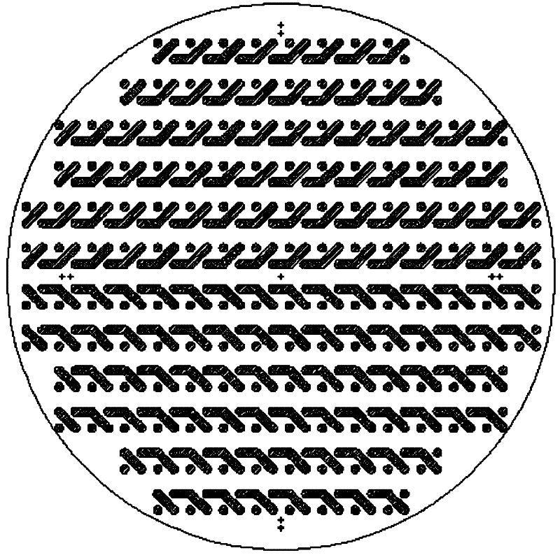
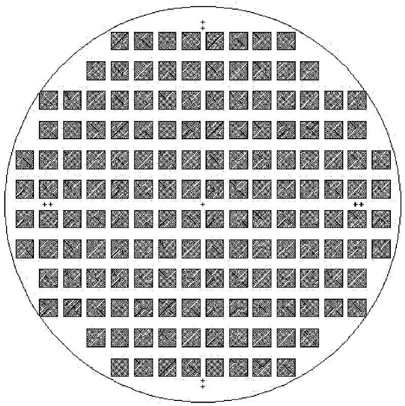
[0016] An electromigration test structure of a through-silicon via metal interconnection line, including a silicon wafer, on which a plurality of through-silicon via units are distributed, figure 1 , 2 and 3 respectively give schematic diagrams of the front side of the silicon wafer, TSVs and the back side of the silicon wafer. Figure 5 a shows the schematic diagram of the results of the TSV unit. The TSV unit includes three TSVs, the first, second and third TSVs h 11 、h 12 、h 13 Connected through the metal layer on the back side of the silicon wafer, the second through-silicon via h 12 and the first TSV h of the subsequent adjacent TSV unit 21 It is connected through the metal layer on the front side of the silicon chip. refer to Figure 4 and 5 , the positive current is applied to the first TSV h of the first TSV unit during the tes...


PUM

PropertyMeasurementUnit
Diameteraaaaaaaaaa

Abstract

The invention discloses an electromigration test structure of a silicon through hole metal interconnection wire, which comprises a silicon wafer provided with a plurality of silicon through hole units; the silicon through hole units comprise three silicon through holes; the first to third silicon through holes are connected through a silicon wafer back metal layer, and the second silicon through hole is connected with the first silicon through hole of the subsequent adjacent silicon through hole unit through a silicon wafer front metal layer; and a probe head of four probes is placed at the front end opening of the third silicon through hole, while the other probe head is placed on the position connected with the first silicon through hole through the front metal layer on the silicon wafer. The test structure can make a test on electromigration performances of various silicon through hole metal interconnection wires, and can cut off some samples connected in series in the test processfor section analysis without influence of continuous test of the rest samples, so that the test structure has the characteristics of low test cost, convenient operation and high test efficiency.

Description

technical field [0001] The invention relates to the field of electronic high-density three-dimensional packaging, in particular to an electromigration reliability test structure in a through-silicon via metal interconnection mode. technical background [0002] Through-Silicon Via (TSV) technology is a vertical interconnection technology in a chip, and its electrical signal passes through the through hole on the silicon chip. Compared with the traditional planar metal wire interconnection technology, TSV technology can significantly It can greatly increase the density of the package, which has the advantages of saving space, reducing signal delay and improving chip performance. [0003] Electromigration is a very important cause of failure of interconnect lines in microelectronic devices. Electromigration can cause opens and shorts in interconnect lines. There have been many studies on the electromigration properties of conventional interconnect metal lines. However, there ...

Claims


Application Information

Patent Timeline
IPC IPC(8): H01L23/544G01R31/28
Inventor 刘胜汪学方吕植成袁娇娇宋斌杨亮
Owner HUAZHONG UNIV OF SCI & TECH
Why Eureka
Try Eureka