Trench metal oxide semiconductor field-effect transistor and manufacturing method for same

An oxide semiconductor and field effect transistor technology, which is applied in semiconductor/solid state device manufacturing, semiconductor devices, electrical components, etc., can solve problems such as limitations that have not been substantially improved, and achieve improved avalanche characteristics, reduced turn-on resistance, The effect of reducing device size

Active Publication Date: 2012-04-04
FORCE MOS TECH CO LTD
View PDF6 Cites 14 Cited by
  • Summary
  • Abstract
  • Description
  • Claims
  • Application Information

AI Technical Summary

Problems solved by technology

and figure 1 compared to, image 3 The trench metal oxide semiconductor field effect transistor in the metal oxide semiconductor field effect transistor is lined with a barrier layer 111 below the metal layer 118', however, the various limitations discussed above have not been substantially improved

Method used


Image

  • Trench metal oxide semiconductor field-effect transistor and manufacturing method for same
  • Trench metal oxide semiconductor field-effect transistor and manufacturing method for same
  • Trench metal oxide semiconductor field-effect transistor and manufacturing method for same

Examples


Embodiment Construction

[0070] The advantages of these and other embodiments of the present invention will be described in detail below in conjunction with the accompanying drawings.

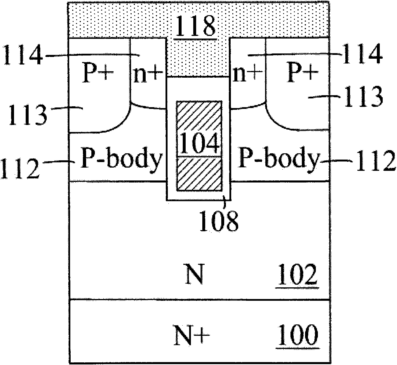
[0071] Figure 5 A three-dimensional view of an N-channel trench MOSFET fabricated on an N+ substrate 200 with a drain deposited on the lower surface of the N+ substrate 200 according to a preferred embodiment of the present invention is disclosed Metal layer 230 . An N-type epitaxial layer 202 is formed on the N+ substrate 200 , and the N-type epitaxial layer 202 includes a plurality of P-type body regions 204 and a plurality of n+ source regions 206 located in the active region. A plurality of first gate trenches 208 extend through the n+ source region 206, the P-type body region 204 and into the N-type epitaxial layer 202, the lower portion of each of the first gate trenches 208 lining There is a first insulating layer 212 as a gate oxide layer and filled with a doped polysilicon layer 210 . Above the second insu...


PUM


Abstract

The invention discloses a trench metal oxide semiconductor field-effect transistor with ultrahigh cell density and a manufacturing method for the same. A source region and a body region are arranged in different areas of a device respectively so that the dimension of the device can be effectively decreased. Besides, trench metallic oxides of the trench metal oxide semiconductor field-effect transistor are in stripe cell structures, so that cell packing density is further increased, and starting resistance between a drain electrode and a source electrode is reduced.

Description

technical field [0001] The invention relates to a device structure and a manufacturing method of a semiconductor power device. In particular, it relates to an improved device structure and fabrication method of a trench metal-oxide-semiconductor field-effect transistor (Metal-Oxide-Semiconductor-Field-Effect-Transistor, MOSFET) with super cell density. Background technique [0002] It is well known that for trench semiconductor power devices, the two parameters, channel packing density (channel width in unit area) and cell density (cell density), are important for improving the performance and cost per unit area of ​​the device. The ratio between them is of great significance, therefore, in the prior art, various structures of trench semiconductor power devices have been proposed in an attempt to obtain higher trench packing density and cell density. [0003] like figure 1 As shown, US Patent No. 6,737,704 discloses an N-channel trench metal-oxide-semiconductor field effec...

Claims


Application Information

Patent Timeline
Patent Type & Authority Applications(China)
IPC IPC(8): H01L29/78H01L29/08H01L21/336
Inventor 谢福渊
Owner FORCE MOS TECH CO LTD
Why Eureka
Try Eureka