LED (Light-Emitting Diode) heat dissipation base plate, LED packaging structure, and manufacturing method of LED heat dissipation base plate and LED packaging structure

A technology for a heat dissipation substrate and a manufacturing method, which is applied in the directions of electrical components, electric solid devices, circuits, etc., can solve the problems of complicated manufacturing process of silicon substrate, unsuitable for popularization and use, complicated design, etc., and achieves clear steps, simple structure, and easy operation. Effect

Active Publication Date: 2013-09-18
常州精睿新能源汽车技术有限公司
View PDF6 Cites 0 Cited by
  • Summary
  • Abstract
  • Description
  • Claims
  • Application Information

AI Technical Summary

Problems solved by technology

However, at present, the production and packaging technology of silicon substrates are basically mastered by foreign companies, and the design is complicated and the cost is high
For example, the manufacturing process of the silicon substrate in the "Using an Etch Stop Layer to Form Through-Wafer Electrical Interconnects and Other Structures" disclosed in the Chinese patent document CN 101517729A and the "Semiconductor Structure with One or More Through Holes" disclosed in the Chinese patent document CN1605126A are both Very complex, correspondingly high cost, not suitable for promotional use

Method used


Image

  • LED (Light-Emitting Diode) heat dissipation base plate, LED packaging structure, and manufacturing method of LED heat dissipation base plate and LED packaging structure
  • LED (Light-Emitting Diode) heat dissipation base plate, LED packaging structure, and manufacturing method of LED heat dissipation base plate and LED packaging structure
  • LED (Light-Emitting Diode) heat dissipation base plate, LED packaging structure, and manufacturing method of LED heat dissipation base plate and LED packaging structure

Examples


Embodiment 1

[0088] (Example 1, LED heat dissipation substrate, using SOI wafer as the base material)

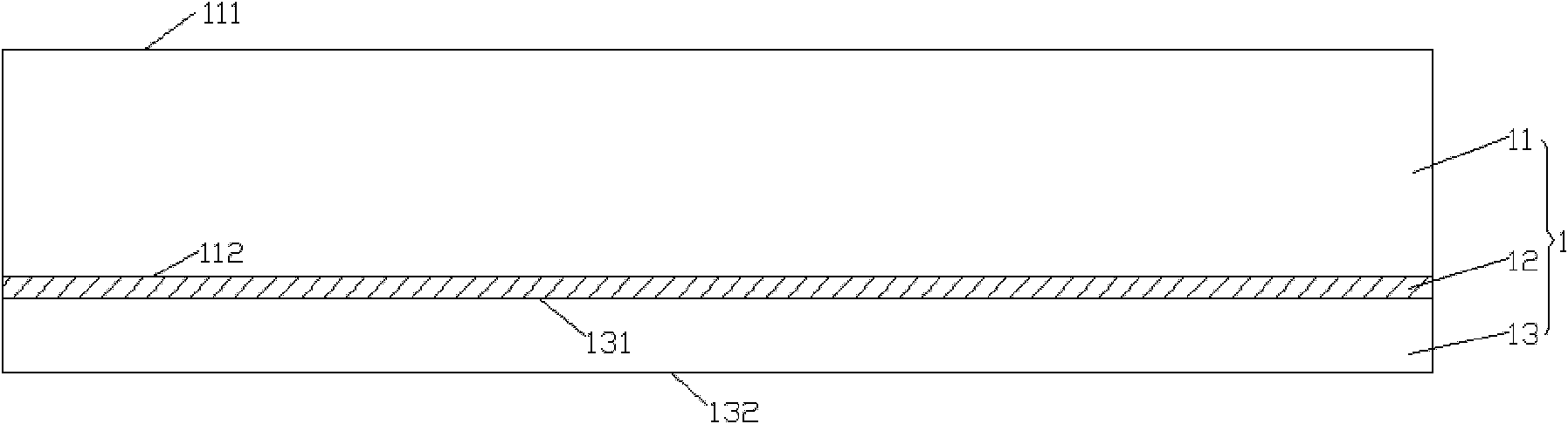
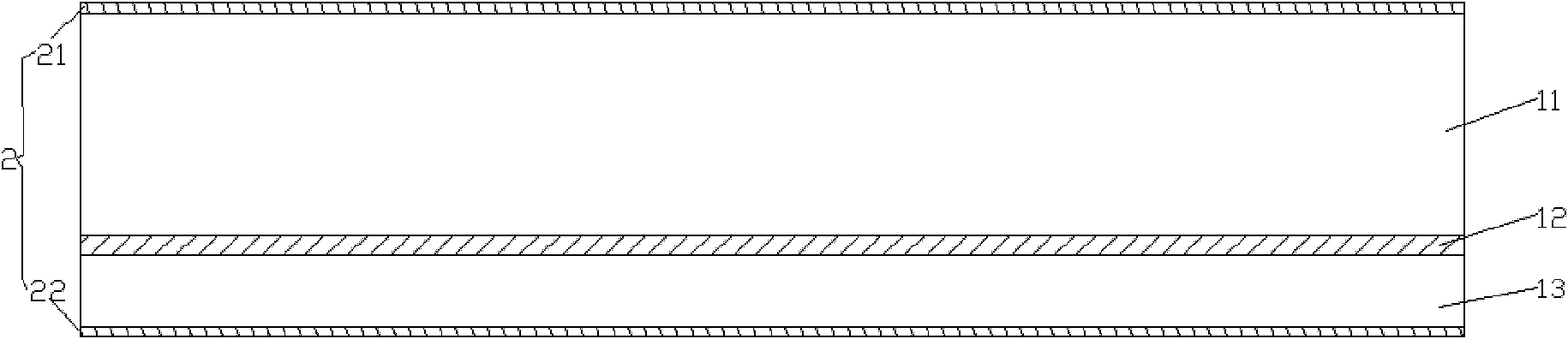
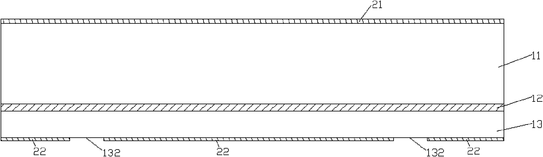
[0089] See Figure 9 , an LED heat dissipation substrate in this embodiment is obtained by etching an SOI wafer 1 as a base material. The structure of the SOI wafer 1 see figure 1 , is an etch stop layer 12 made of silicon dioxide between the upper layer 11 and the bottom layer 13 made of silicon. The thickness of the upper layer 11 is 300-500um; the thickness of the etching stop layer 12 is 1-2um, which is sufficient to resist the double-side etching operation; the thickness of the bottom layer 13 is 50-200um.

[0090] Such as Figure 9 As shown, the specific structure of the LED heat dissipation substrate is: an upper layer 11 of silicon material, which includes a silicon cup 4 formed by etching to the etching stop layer 12; an etching stop layer of silicon dioxide material located on the lower surface of the upper layer 11 12. A bottom layer 13 made of silicon, including at least ...

Embodiment 2

[0091] (Example 2, LED heat dissipation substrate, using SOI wafer as the base material)

[0092] See Figure 10 On the basis of Embodiment 1, the LED heat dissipation substrate of this embodiment further includes an adhesive layer 6 made of Sn / Au alloy or silver paste on the bottom of the silicon cup 4 and the lower surface of the bottom layer 13 . Wherein the adhesive layer 6 at the bottom of the silicon cup 4 is used to bind the high-power LED chip 7; the adhesive layer 6 on the lower surface of the bottom layer 13 is used to connect with other circuit boards to form an effective mechanical binding and heat conduction path .

Embodiment 3

[0093] (Example 3, LED heat dissipation substrate, using a single crystal silicon wafer as the base material)

[0094] See Figure 21 , an LED heat dissipation substrate in this embodiment is obtained by etching a single crystal silicon wafer 20 as a base material. Specific structural parts of the monocrystalline silicon wafer 20 Figure 13 , including a first surface 201 and a second surface 202 .

[0095] Such as Figure 21 As shown, the specific structure of the LED heat dissipation substrate is: a silicon cup 4 formed by etching on the first surface 201; at least two guide holes 3 formed by etching on the second surface 202; the guide holes 3 are filled with metal conductors 5. The diameter of the upper end surface 31 of the guide hole 3 is ≥100um, which is used for welding the pins of high-power LED chips. The depth of the guide hole 3 is 50-200um. The guide hole 3 can be in various shapes, such as square, rectangle, trapezoid, etc. Moreover, the number of the guide ...


PUM


Abstract

The invention discloses an LED (Light-Emitting Diode) heat dissipation base plate, an LED packaging structure and a manufacturing method of the LED heat dissipation base plate and the LED packaging structure. An SOI (Silicon-On-Insulator) wafer or a monocrystalline silicon wafer is taken as a substrate. The heat dissipation base plate taking the SOI wafer as the substrate comprises an upper layer made of silicon materials, an etching stopping layer made of silicon dioxide materials and a bottom layer made of the silicon materials, wherein the upper layer comprises a silicon cup formed by etching; the etching stopping layer is positioned in the SOI wafer below the upper layer; and the bottom layer comprises at least two guide holes formed by etching. The heat dissipation base plate taking the monocrystalline silicon wafer as the substrate comprises a silicon cup, at least two guide holes and metal conductors, wherein the silicon cup is formed by etching on a first surface; the guide holes are formed by etching on a second surface; and the metal conductors are filled in the guide holes. The invention has the beneficial effects that a silicon-manufactured base plate is adopted to replace the existing various ceramic heat dissipation base plates; the structure is simple; not only can the purpose of highly-efficient heat dissipation be achieved, but also the basic production cost can be greatly reduced; and meanwhile, as the thermal expansion coefficient of a silicon is close to that of an LED chip substrate, the service life of an LED chip is facilitated to be prolonged.

Description

technical field [0001] The invention relates to the field of LED semiconductors, in particular to a heat dissipation substrate for packaging high-power LED chips, an LED packaging structure using the heat dissipation substrate, and a manufacturing method for the two. Background technique [0002] With the rising awareness of global environmental protection and the rapid progress of optoelectronic technology, the LED semiconductor lighting industry with energy saving, power saving, high efficiency, fast response time, long life cycle, and mercury-free is rapidly becoming one of the hottest industries. At present, low-power LED light-emitting diode chips have been widely used in display screens, backlights for LCD TVs and computer screens, as well as interior decoration and general lighting. However, the largest market for LEDs in the future is street lighting, and this application requires the use of high-power, high-brightness LED chips, and has high requirements for the ove...

Claims


Application Information

Patent Timeline
Patent Type & Authority Patents(China)
IPC IPC(8): H01L33/00H01L33/64
CPCH01L2224/48091H01L2224/73265H01L2924/181
Inventor 刘红兵
Owner 常州精睿新能源汽车技术有限公司
Why Eureka
Try Eureka