Target power loading method, target power supply and semiconductor processing equipment

A target material and power supply technology, which is applied in the field of microelectronics, can solve problems such as impossibility, and achieve the effects of increasing metal ionization rate, maintaining process continuity, and avoiding a sharp increase in heat generation

Inactive Publication Date: 2012-04-11
BEIJING NAURA MICROELECTRONICS EQUIP CO LTD
View PDF3 Cites 4 Cited by
  • Summary
  • Abstract
  • Description
  • Claims
  • Application Information

AI Technical Summary

Problems solved by technology

This metal ionization rate can meet the needs of today's industrial processing to a certain extent. However, some high-tech companies today have achieved processing accuracy of 32nm level. It is conceivable that the microelectronics processing industry will enter a new era in the near future. In the 32nm era, in order to realize this new technology node, it is required that the metal ionization rate in the sputtering process of the copper interconnection layer reach a level of 80% or higher under the premise of ensuring process stability and controllability However, as far as the existing technology and equipment are concerned, it is obviously impossible to achieve the above requirements

Method used


Image

  • Target power loading method, target power supply and semiconductor processing equipment
  • Target power loading method, target power supply and semiconductor processing equipment
  • Target power loading method, target power supply and semiconductor processing equipment

Examples


Embodiment Construction

[0030] In order for those skilled in the art to better understand the technical solution of the present invention, the target power loading method, target power supply and semiconductor processing equipment using the above-mentioned target power loading method / target power supply provided by the present invention will be described below in conjunction with the accompanying drawings Describe in detail.

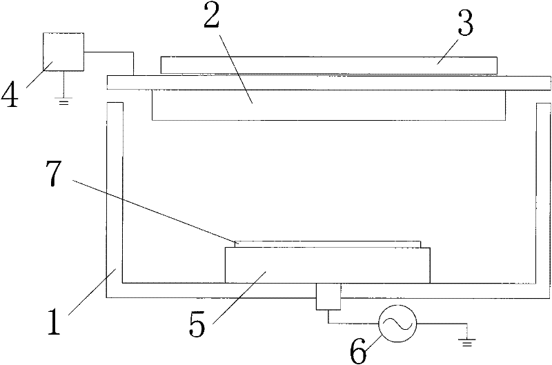
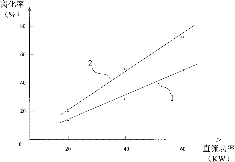
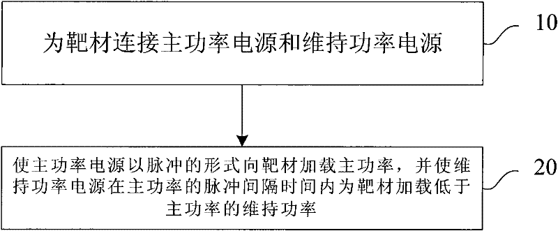
[0031] see image 3 , is a schematic flowchart of the target power loading method provided by the present invention. The target power loading method is mainly used to load power to the target in the magnetron sputtering process, which includes the following steps: 10) connecting the main power supply and the maintenance power supply for the target; 20) making the main power supply with A certain main power is applied to the target in the form of a pulse. The action time of a single pulse is t1, and the pulse interval is t2. When the main power is large enough, the metal ioniza...


PUM

PropertyMeasurementUnit
frequencyaaaaaaaaaa

Abstract

The invention provides a target power loading method for a magnetic control sputtering process, which comprises the following steps that: (10) a target is respectively connected with a main power supply and a maintenance power supply; and (20) a certain main power is loaded to the target by the main power supply in a pulse form, so that the maintenance power supply at least loads a certain maintenance power to the target during pulse interval time of the main power supply, the maintenance power is less than the main power, and further, the glow discharge process of the sputtering process is maintained during the pulse interval time of the main power. By the target power loading method disclosed by the invention, the stability and the controllability of the process are ensured, simultaneously, the metal ionization is remarkably improved, and further, the process requirements of the technical node are met. In addition, the invention also provides a target power supply which comprises a main power module and a maintenance power module, and semiconductor processing equipment which applies the target power loading method or the target power supply.

Description

technical field [0001] The present invention relates to the technical field of microelectronics, in particular, to a target power loading method, a target power supply, and semiconductor processing equipment using the above target power loading method / target power supply. Background technique [0002] In modern industry, microelectronic processing technology has made unprecedented achievements. Among them, large-scale integrated circuits have been applied to various fields in people's production and life. At the same time, the manufacturing process and processing equipment of integrated circuits are also being continuously improved and updated at an astonishing speed. [0003] Magnetron sputtering is a key technology used to prepare metal interconnect layers such as copper / aluminum in integrated circuits. In the magnetron sputtering process, part of the target atoms are sputtered out of the target surface in the form of ions. Usually, the proportion of the metal particles ...

Claims


Application Information

Patent Timeline
Patent Type & Authority Applications(China)
IPC IPC(8): C23C14/35
CPCC23C14/35H01J37/3408C23C14/3485H01J37/3467
Inventor 杨柏夏威
Owner BEIJING NAURA MICROELECTRONICS EQUIP CO LTD
Why Eureka
Try Eureka