Method for improving tensile stress of silicon nitride film in semiconductor devices

A technology of silicon nitride thin film and tensile stress, applied in semiconductor/solid-state device manufacturing, electrical components, circuits, etc.

Inactive Publication Date: 2012-04-11
SHANGHAI HUALI MICROELECTRONICS CORP
View PDF3 Cites 4 Cited by
  • Summary
  • Abstract
  • Description
  • Claims
  • Application Information

AI Technical Summary

Problems solved by technology

In order to obtain a silicon nitride film with higher tensile stress, as shown in Figure 1, plasma treatment under a nitrogen atmosphere or ultraviolet light irradiation is usually used to remove a certain amount of hydr

Method used


Image

  • Method for improving tensile stress of silicon nitride film in semiconductor devices
  • Method for improving tensile stress of silicon nitride film in semiconductor devices
  • Method for improving tensile stress of silicon nitride film in semiconductor devices

Examples


Embodiment Construction

[0017] The main process of the preferred embodiment of the method for improving the tensile stress of the silicon carbide film of the present invention is as follows:

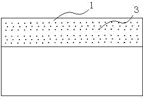
[0018] In the process of depositing the silicon nitride film, a certain amount of organic pore former 3 is added to the silicon nitride film 1, and the organic pore former 3 here is alpha-terpinene (ATRP) or norbornadiene (BCHD). ), etc., such as Figure 2A shown;

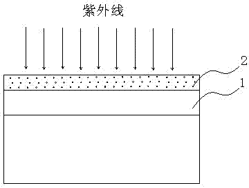
[0019] When the film 1 is irradiated with ultraviolet light, part of the Si-H / N-H bonds in the silicon nitride film 1 will break and shrink after obtaining energy. A certain content of hydrogen 2 in film 1, such as Figure 2B shown, and it is known through experiments that the tensile stress of the film is proportional to the shrinkage rate of the film. The data results can be found in image 3 shown, thereby increasing the tensile stress of the silicon nitride film.

[0020] Applying the thin film preparation method to the etch stop layer of th...


PUM


Abstract

The invention discloses a method for improving tensile stress of a silicon nitride film in semiconductor devices. The method comprises the following steps of adding a certain quantity of organic pore-forming agent into the silicon nitride film while depositing the silicon nitride film; irradiating the silicon nitride film with UV-light, wherein part of Si-H/N-H bonds in the silicon nitride film crack and shrink after obtaining energy, and because of volatilization of the organic pore-forming agent, the shrink of the film is enhanced; the organic pore-forming agent is Alpha-terpinene or NBDNorbornadiene. The film preparation method is applied in a CESL (contact etch stop layer) layer of CMOS (Complementary Metal-Oxide-Semiconductor Transistor)production and can improve the performance of NMOS (PMOS (N-channel Metal Oxide Semiconductor) devices.

Description

technical field [0001] The present invention generally relates to the technical field of integrated circuit manufacturing, and more particularly, the present invention relates to a method for increasing the tensile stress of silicon nitride films in semiconductor devices. Background technique [0002] As the feature line width of integrated circuits is reduced to less than 90nm, improving device performance through gate thickness, gate dielectric constant and junction depth can no longer meet the requirements of the process. Even if the gate thickness is controlled at 5 atomic layers, the junction depth is also Only 10nm. To meet the requirement of switching speed, high-stress silicon nitride technology has been widely studied. With the high stress applied by silicon nitride on the gate mechanism, the carrier mobility of MOS devices can be greatly improved. Specifically, the compressive stress on the PMOS structure can improve the mobility of holes, while the tensile stress...

Claims


Application Information

Patent Timeline
IPC IPC(8): H01L21/8238H01L21/318
Inventor 徐强张文广郑春生陈玉文
Owner SHANGHAI HUALI MICROELECTRONICS CORP
Why Eureka
Try Eureka