Production process of aluminum pad based on polyimide matrix
A technology of polyimide substrate and polyimide layer, which is applied in the manufacture of semiconductor/solid-state devices, electric solid-state devices, semiconductor devices, etc. Effects of damage, reduction of the possibility of collapse of narrow aluminum wires
- Summary
- Abstract
- Description
- Claims
- Application Information
AI Technical Summary
Problems solved by technology
Method used
Image

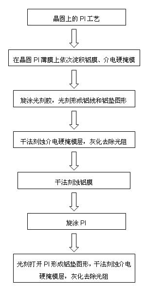
Examples
Embodiment 1
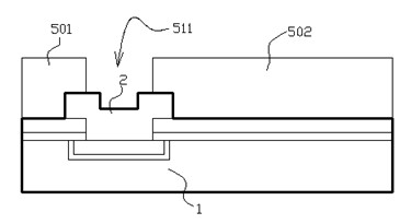
[0028] see figure 2 , the first polyimide layer 5 is covered on the semiconductor device wafer 1, and the polyimide adopts polyaddition polyimide. The first polyimide layer is etched to form a first opening 511 , and the first polyimide layer 5 is divided into left and right first polyimide blocks 501 , 502 . In the first opening 511, the aluminum pad 2 used as the signal connection terminal of the semiconductor device is exposed therein.
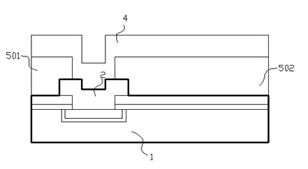
[0029] Deposit a layer of aluminum film on the first polyimide layer 501, 502, part of the aluminum film is deposited in the first opening 511 and cover the aluminum pad 2 at the same time, and the aluminum pad 2 and the aluminum film layer 4 are connected into one piece , the obtained wafer structure is as image 3 shown.
[0030] see Figure 4 , on the aluminum film layer 4, a dielectric hard mask layer 3 is deposited by low pressure chemical vapor deposition. The dielectric hard mask layer 3 consists of SiO 2 and SiN hybrid materi...
Embodiment 2
[0036] see figure 2 , a large number of semiconductor devices are arranged on the wafer 1. First, a first polyimide layer 5 is covered on the wafer 1. The polyimide is a mixture of polyaddition polyimide and polycondensation polyimide. . The first polyimide layer is etched to form a first opening 511 , and the first polyimide layer 5 is divided into first polyimide blocks 501 , 502 . In the first opening 511, the aluminum pad 2 used as the signal connection terminal of the semiconductor device is exposed therein.
[0037] Deposit a layer of aluminum film on the first polyimide layer 501, 502, part of the aluminum film is deposited in the first opening 511 and cover the aluminum pad 2 at the same time, and the aluminum pad 2 and the aluminum film layer 4 are connected into one piece , the obtained wafer structure is as image 3 shown.
[0038] see Figure 4 , on the aluminum film layer 4, a dielectric hard mask layer 3 is deposited by plasma-enhanced chemical vapor deposi...
PUM
| Property | Measurement | Unit |
|---|---|---|
| Thickness | aaaaa | aaaaa |
| Thickness | aaaaa | aaaaa |
Abstract
Description
Claims
Application Information
 - R&D
- Intellectual Property
- Life Sciences
- Materials
- Tech Scout
- Unparalleled Data Quality
- Higher Quality Content
- 60% Fewer Hallucinations
Browse by: Latest US Patents, China's latest patents, Technical Efficacy Thesaurus, Application Domain, Technology Topic, Popular Technical Reports.
© 2025 PatSnap. All rights reserved.Legal|Privacy policy|Modern Slavery Act Transparency Statement|Sitemap|About US| Contact US: help@patsnap.com