

Manufacturing method of twin-transistor and zero-capacitance dynamic RAM (Random Access Memory)
A dual-transistor and MOS transistor technology, applied in the field of preparation of dual-transistor zero-capacitance dynamic RAM, can solve problems such as unresolved manufacturability
- Summary
- Abstract
- Description
- Claims
- Application Information
AI Technical Summary
Problems solved by technology
Method used
Image

Examples
preparation example Construction
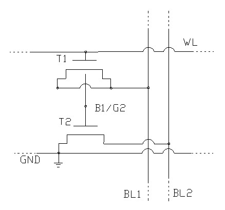
[0051] The present invention is a method for preparing silicon-on-insulator gate-back dual-transistor zero-capacitance dynamic RAM with manufacturability design, wherein the dual transistors are two cascaded MOS transistors T1 and T2 formed on a common substrate, specifically Including preparatory procedures and subsequent procedures, wherein the preparatory procedures include:
[0052] Thin oxide layers are respectively formed on the channel surfaces between the respective source and drain electrodes of T1 and T2;
[0053] The respective gate trenches of T1 and T2 are respectively formed by additional sample gate wet etch-back on the thin oxide layer, and the high dielectric layer and the metal oxide above it are respectively formed in the respective gate trenches of T1 and T2 layer of dielectric material. Optionally, the high dielectric layer and the metal oxide dielectric material layer can also be formed first when the sample gate is prepared, and not removed when the add...
Embodiment 1
[0059] Embodiment one , when the two cascaded MOS transistors T1 and T2 are all NMOS structures, specifically include the following steps:
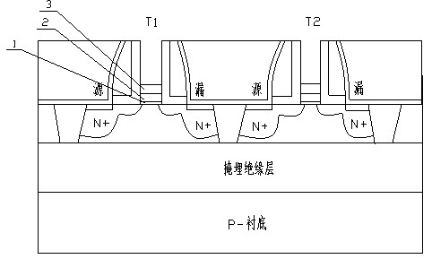
[0060] Such as Figure 3A As shown, the gate trenches of T1 and T2 are respectively formed by additional sample gate wet etch back, and the gate dielectric layers of T1 and T2 include high dielectric layer 2 (HK layer) and metal oxide dielectric material above it Layer 3 (Cap layer), a thin oxide layer 1 can optionally be grown under the high dielectric layer 2, and the gate dielectric layer of T1 and T2 can be formed after the sample gate is wet-etched back, or it can be formed during the preparation of the sample gate Formed and not removed during sample gate wet etch back;
[0061] Such as Figure 3B As shown, perform photolithography, open the window in the T1 region, close the window in the T2 region, perform an angle tilt, rotate 180 degrees, and then perform bidirectional ion implantation so that the gate is close to the source...
Embodiment 2
[0066] Embodiment two, When the two cascaded MOS transistors T1 and T2 are all PMOS structures, the following steps are specifically included:
[0067] Such as Figure 5A As shown, the gate trenches of T1 and T2 are respectively formed by additional sample gate wet etch back, and the gate dielectric layers of T1 and T2 include high dielectric layer 2 (HK layer) and metal oxide dielectric material above it Layer 3 (Cap layer), a thin oxide layer 1 can optionally be grown under the high dielectric layer 2, and the gate dielectric layer of T1 and T2 can be formed after the sample gate is wet-etched back, or it can be formed during the preparation of the sample gate Formed and not removed during sample gate wet etch back;
[0068] Such as Figure 5B As shown, perform photolithography, open the window in the T1 area, close the window in the T2 area, perform an angle tilt, rotate 180 degrees, and then perform bidirectional ion implantation to make the gate close to the source an...
PUM
 Abstract
Description
Claims
Application Information