Germanium-silicon heterojunction bipolar transistor and manufacturing method thereof

A heterojunction bipolar, transistor technology, used in semiconductor/solid-state device manufacturing, semiconductor devices, electrical components, etc., can solve the problems of high research and development costs of advanced processes, toxic compound semiconductors, and difficulty in achieving characteristic frequencies, and achieves suppression of Current edge set effect, reduce collector resistance, improve the effect of BVCEO

Active Publication Date: 2012-04-18
SHANGHAI HUAHONG GRACE SEMICON MFG CORP
View PDF3 Cites 3 Cited by
  • Summary
  • Abstract
  • Description
  • Claims
  • Application Information

AI Technical Summary

Problems solved by technology

[0002] In radio frequency applications, higher and higher device characteristic frequencies are required. Although RFCMOS can achieve higher frequencies in advanced process technologies, it is still difficult to fully meet radio frequency requirements. For example, it is difficult to achieve characteristic frequencies above 40GHz,

Method used


Image

  • Germanium-silicon heterojunction bipolar transistor and manufacturing method thereof
  • Germanium-silicon heterojunction bipolar transistor and manufacturing method thereof
  • Germanium-silicon heterojunction bipolar transistor and manufacturing method thereof

Examples


Embodiment Construction

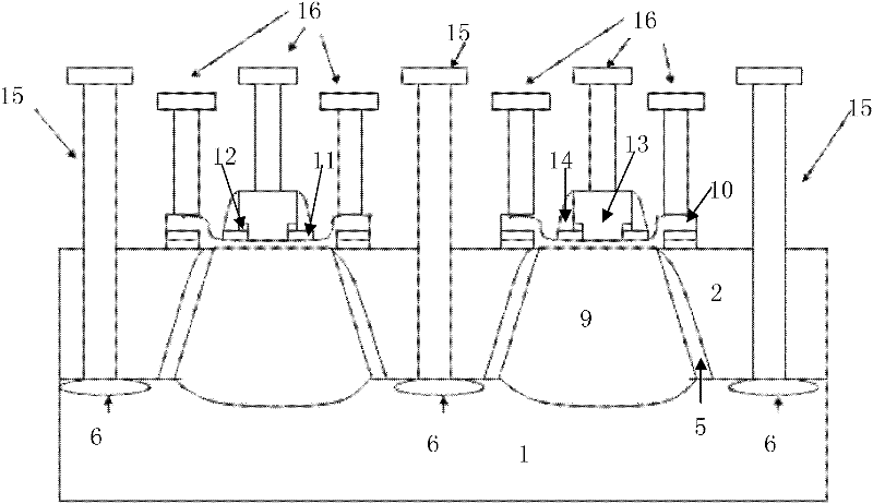
[0044] like figure 1 Shown is a schematic diagram of the structure of a germanium-silicon heterojunction bipolar transistor according to an embodiment of the present invention. The germanium-silicon heterojunction bipolar transistor in the embodiment of the present invention is formed on a P-type silicon substrate 1, and the isolation structure of the active region is a shallow trench isolation 2. The germanium-silicon heterojunction bipolar transistor includes:

[0045] A collector region 9 is composed of an N-type ion implantation region formed in the active region, and the depth of the collector region 9 is greater than the depth of the bottom of the shallow trench isolation 2 .

[0046] A pseudo-buried layer (NBL) 6, composed of arsenic ion implantation regions formed at the bottom of the shallow trench isolation 2 on both sides of the active region, the pseudo-buried layer 6 extends into the active region and connects with the The collector region 9 is in contact with ea...


PUM

PropertyMeasurementUnit
Thicknessaaaaaaaaaa
Thicknessaaaaaaaaaa
Thicknessaaaaaaaaaa

Abstract

The invention discloses a germanium-silicon heterojunction bipolar transistor. A base region is composed of three layers of structures including a silicon buffering layer, a germanium-silicon layer and a silicon cap layer. An accelerating field of electrons is formed in the base region by the germanium-silicon layer to improve the frequency response of a device. The silicon cap layer can be used for optimizing the position of an emission junction, reducing a recombination current of the base region and improving the linearity and a BVCEO (Breakdown Voltage ceo) of the device. A collector electrode is led out from shallow slot isolation through a fake buried layer and a deep hole contact so that the resistance of the collector electrode can be reduced and the frequency response of the device can be improved. The fake buried layer is doped by arsenic so that the cross diffusion of the fake buried layer can be effectively controlled, the parasitic capacitance is reduced and the frequencyresponse of the device is improved. An emission region is of a narrow emission electrode structure and can be used for inhibiting a current crowding effect and improving a current density in a unit area. One silicon oxidation layer is formed on a contact position between the emission region and the base region so that a barrier height of the emission junction can be improved and the injection frequency of the emission junction is improved. The invention further discloses a manufacturing method of the germanium-silicon heterojunction bipolar transistor.

Description

technical field [0001] The invention relates to the field of semiconductor integrated circuit manufacturing, in particular to a germanium-silicon heterojunction bipolar transistor; the invention also relates to a manufacturing method of the germanium-silicon heterojunction bipolar transistor. Background technique [0002] In radio frequency applications, higher and higher device characteristic frequencies are required. Although RFCMOS can achieve higher frequencies in advanced process technologies, it is still difficult to fully meet radio frequency requirements. For example, it is difficult to achieve characteristic frequencies above 40GHz, and advanced technology The research and development cost of compound semiconductors is also very high; compound semiconductors can realize very high characteristic frequency devices, but due to the disadvantages of high material cost and small size, and the toxicity of most compound semiconductors, its application is limited. Silicon ge...

Claims


Application Information

Patent Timeline
IPC IPC(8): H01L29/737H01L29/06H01L21/331
Inventor 陈帆薛恺陈雄斌周正良潘嘉李昊周克然陈曦蔡莹
Owner SHANGHAI HUAHONG GRACE SEMICON MFG CORP
Why Eureka
Try Eureka