Silicon carbide avalanche photoelectric detector provided with graphene transparent electrode

A transparent electrode, avalanche photoelectric technology, applied in circuits, photovoltaic power generation, electrical components, etc., can solve the problems of uneven distribution of the interface electric field to the light signal of the electrode, reduce the detectability of the device, and large power consumption of the device, and achieve the suppression of electric field concentration. Side effect, improve detection sensitivity, prevent premature breakdown

Inactive Publication Date: 2018-06-29
XIAMEN UNIV
View PDF6 Cites 13 Cited by
  • Summary
  • Abstract
  • Description
  • Claims
  • Application Information

AI Technical Summary

Problems solved by technology

However, for silicon carbide avalanche photodetectors, the avalanche breakdown voltage is very high, and the power consumption of the device is relatively large.
In addition, due to the difficulty in the design of the P-type ohmic contact electrode, such as the inconsistency of the contact between the electrode metal and the silicon carbide surface, the uneven distribution of the interface electric field and the blocking effect of the electrode on the optical signal further reduce the detectability of the device.

Method used


Image

  • Silicon carbide avalanche photoelectric detector provided with graphene transparent electrode

Examples


Embodiment Construction

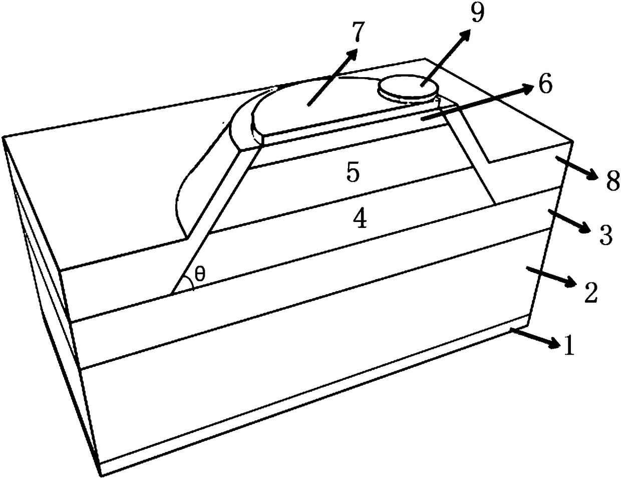
[0012] The specific embodiment of the present invention is as figure 1 shown in commercially available low resistivity N + On the type 4H-SiC substrate 2, the first N-type epitaxial buffer layer 3, N - Type epitaxial absorption layer 4, the second N type epitaxial multiplication layer 5 and P + Type ohmic contact layer 6. The thickness and doping concentration of the first N-type epitaxial buffer layer may be 0.1 μm and 5×10 18 / cm 3 , N - The thickness and doping concentration of the epitaxial absorber layer can be 1.0 μm and 1×10 15 / cm 3 , The thickness and doping concentration of the second N-type epitaxial multiplication layer can be 0.2um and 1×10 18 / cm 3 ,P + The thickness and doping concentration of the type ohmic contact layer can be 0.2μm and 1×10 19 / cm 3 . RCA standard cleaning was performed on the above 4H-SiC, and the epitaxial wafer P + A graphene film 7 is formed on the surface of the type ohmic contact layer as P + type ohmic contact electrodes....


PUM


Abstract

The invention discloses a silicon carbide avalanche photoelectric detector provided with a graphene transparent electrode and relates to a semiconductor photoelectric detector. The silicon carbide avalanche photoelectric detector is provided with a substrate, wherein a first N type epitaxial buffer layer, an N type epitaxial absorption layer, a second N<-> type epitaxial multiplication layer and aP<+> type ohmic contact layer which are homogeneous are sequentially arranged on the substrate; and multiple graphene transparent electrode layers grow on the surface of the P<+> type ohmic contact layer by virtue of an electrothermal decomposition process, and one height from the surface of a graphene layer to the surface of the first N type epitaxial buffer layer is etched by adopting a photolithography mask technology and an ICP etching process, so that the P<+> type ohmic contact layer, the second N type epitaxial multiplication layer and the N- type epitaxial absorption layer are circular truncated cones; and one compact SiOx/Si3N4 protection passivation layer is grown by virtue of a plasma enhanced chemical vapor deposition process. An N type ohmic contact electrode is sputtered onthe back of an N+ type substrate, and a bonding pad window is etched by virtue of a photolithography technology and a bonding pad for the graphene transparent electrode layers is prepared on the SiOx/Si3N4 protection passivation layer.

Description

technical field [0001] The invention relates to a semiconductor photodetector, in particular to a silicon carbide avalanche photodetector with a graphene transparent electrode having a detection wavelength of 200-400 nm. Background technique [0002] The preparation of high-performance sun-blind (detection wavelength 250-280nm) ultraviolet photodetectors is of great value in many special fields, such as missile exhaust detection, high-voltage leakage monitoring, flame sensors, non-line-of-sight ultraviolet communication, etc. The detection of deep ultraviolet with a wavelength of less than 250nm is also very important in the application of fluorescence Raman spectroscopy; in addition, the detection of near ultraviolet bands from 300nm to 400nm is also very extensive, especially in medical imaging and nuclear energy detection, the detection of ultraviolet light of weak ultraviolet signals Detectors have become a research hotspot in the field of photoelectric detection in the ...

Claims


Application Information

Patent Timeline
Patent Type & Authority Applications(China)
IPC IPC(8): H01L31/0216H01L31/0224H01L31/0236H01L31/107
CPCY02E10/50H01L31/107H01L31/02161H01L31/022408H01L31/022466H01L31/02363
Inventor 洪荣墩吴正云林鼎渠张志威孙存志
Owner XIAMEN UNIV
Why Eureka
Try Eureka