Time-interleaving analogue-to-digital converter capable of suppressing sampling time mismatching

An analog-to-digital converter and time-interleaving technology, which is applied in the field of structure design of time-interleaving analog-to-digital converters, can solve the problems of increasing the relative error of the signal bandwidth, increasing the on-resistance and parasitic capacitance of the signal path, and increasing the bandwidth mismatch.

Inactive Publication Date: 2012-04-18
UNIV OF ELECTRONICS SCI & TECH OF CHINA
View PDF3 Cites 29 Cited by
  • Summary
  • Abstract
  • Description
  • Claims
  • Application Information

AI Technical Summary

Problems solved by technology

[0007] 1. The introduction of the front switch will increase the on-resistance and parasitic capacitance of the signal path, reduce the bandwidth of the input signal, increase the relative error of the signal bandwidth, and further intensify the impact of bandwidth mismatch
[0008] 2. The sampling time is determined by the main clo

Method used


Image

  • Time-interleaving analogue-to-digital converter capable of suppressing sampling time mismatching
  • Time-interleaving analogue-to-digital converter capable of suppressing sampling time mismatching
  • Time-interleaving analogue-to-digital converter capable of suppressing sampling time mismatching

Examples


Embodiment Construction

[0019] The present invention will be further described below in conjunction with the figures.

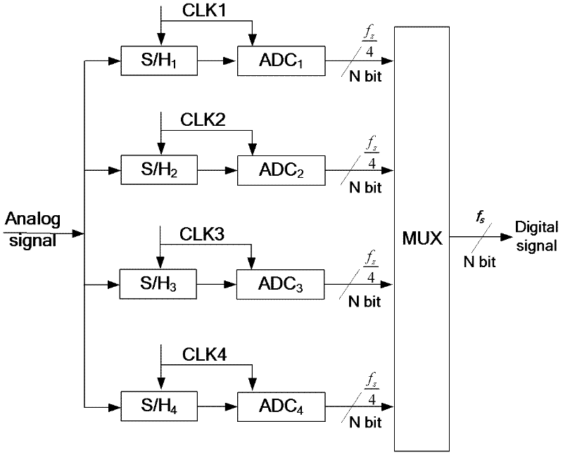
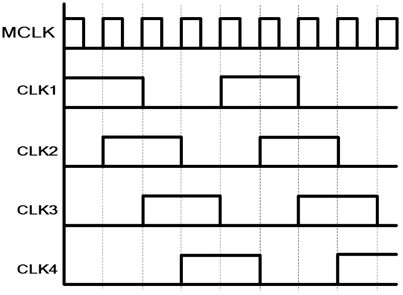
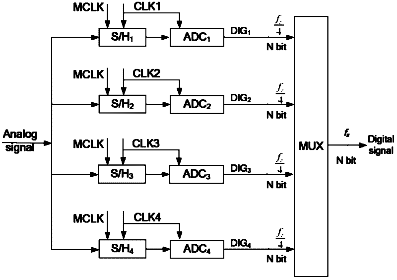
[0020] Such as image 3 Shown is the four-channel time interleaved analog-to-digital converter proposed by the present invention, and its timing diagram is as follows Figure 4 Shown. Figure 4 In, the duty cycle of each channel clock is 25%, and in each sampling clock phase, there is always only one channel sampling, so the input signal load is reduced and the input bandwidth is increased. Compared to traditional time-interleaved analog-to-digital converters (such as figure 1 Shown), image 3 The sampling and holding circuit of each channel is controlled by the channel clock CLKi (i means different channels, i=1, 2, 3, 4) and the master clock MCLK, and the sampling time of each channel is determined by MCLK. The specific working method takes channel one as an example, and the other channels work in the same manner.

[0021] The sample and hold circuit structure of channel one is as foll...


PUM


Abstract

The invention discloses a time-interleaving analogue-to-digital converter capable of suppressing sampling time mismatching, and relates to the technical field of micro-electronics. The invention provides the structure of the time-interleaving analogue-to-digital converter capable of suppressing the sampling time mismatching aiming at the influence of the sampling time mismatching on the time-interleaving analogue-to-digital converter. The analogue-to-digital converter comprises a channel sampling and holding circuit, a sub-analogue-to-digital converter and a multiplexor. The channel sampling and holding circuit introduces a system main clock to determine a sampling time, so that the sampling time mismatching caused by sampling by each channel respectively is avoided, and the dynamic performance of the time-interleaving analogue-to-digital converter is improved effectively. In the method, the sampling and holding circuit does not need to be preposed, so that influence on an input signal bandwidth is avoided; moreover, the influence of charge injection is eliminated and the linearity of a system is improved by utilizing a lower pole plate sampling technology by the channel sampling and holding circuit.

Description

Technical field [0001] The invention relates to an analog-to-digital converter in microelectronics technology, in particular to a structural design of a time-interleaved analog-to-digital converter that can suppress sampling time mismatch. Background technique [0002] Analog-to-digital converter is a tool for converting analog signals into digital signals. As an interface between analog technology and digital technology, it is widely used in industrial control, radar, communications, consumer electronics and other fields. It plays an important role in information technology. effect. With the continuous improvement of integrated circuit manufacturing technology and the introduction of new materials, the digital signal processing technology continues to advance, which puts forward higher requirements on the speed of the analog-to-digital converter. [0003] One of the most popular ways to increase the speed of analog-to-digital converters is to use multiple analog-to-digital conver...

Claims


Application Information

Patent Timeline
IPC IPC(8): H03M1/12
Inventor 李靖宁宁吴霜毅于奇眭志凌宋文青朱欢倪春晓朱波
Owner UNIV OF ELECTRONICS SCI & TECH OF CHINA
Why Eureka
Try Eureka