Self-alignment channel doping for restraining CMOS (Complementary Metal Oxide Semiconductor) short channel effect and preparation method thereof

A short channel effect and channel doping technology, which is applied in semiconductor/solid-state device manufacturing, electrical components, circuits, etc., can solve the problem of increasing source-substrate junction depth Xj, affecting source-substrate, and increasing source-drain parasitic resistance and other problems to achieve the effect of suppressing short channel effect and improving performance

Inactive Publication Date: 2012-04-25
SHANGHAI HUALI MICROELECTRONICS CORP
View PDF3 Cites 1 Cited by
  • Summary
  • Abstract
  • Description
  • Claims
  • Application Information

AI Technical Summary

Problems solved by technology

[0007] The invention discloses a self-aligned channel doping to suppress the CMOS short channel effect and a preparation method thereof, which are used to solve the problems in the prior art: 1. The source-drain doping will be compensated, resulting in an increase in the parasitic resistance of the source-drain ; 2. It will affect the profile of the source lining and drain lining PN junction, causing their reverse bias leakage current to increase; 3. It may increase the junction depth Xj of the source lining and drain lining PN junction, which will have a negative effect on suppressing SCE question

Method used


Image

  • Self-alignment channel doping for restraining CMOS (Complementary Metal Oxide Semiconductor) short channel effect and preparation method thereof
  • Self-alignment channel doping for restraining CMOS (Complementary Metal Oxide Semiconductor) short channel effect and preparation method thereof
  • Self-alignment channel doping for restraining CMOS (Complementary Metal Oxide Semiconductor) short channel effect and preparation method thereof

Examples


Embodiment Construction

[0035] The specific embodiments of the present invention will be further described below in conjunction with the accompanying drawings:

[0036] A self-aligned channel doping suppresses CMOS short channel effect and a preparation method thereof, wherein:

[0037] A back gate high dielectric constant CMOS structure including a first transistor 110 and a second transistor 120 is formed on a silicon substrate; wherein, the substrate is set as a P-type silicon substrate.

[0038] Further, the first transistor 110 is set as an NMOS tube, and the second transistor 120 is set as a PMOS tube.

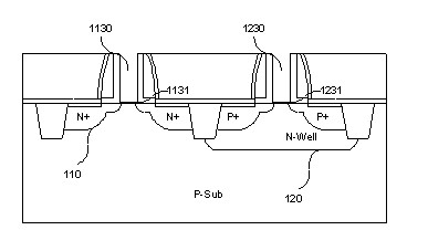
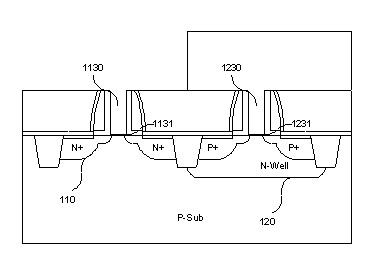
[0039] figure 2 It is the structural schematic diagram of the self-aligned channel doping suppressing CMOS short channel effect and the preparation method of the present invention after step a, please refer to figure 2 , Step a: Remove the sample gate in the first transistor gate trench 1130 of the first transistor 110 device and the second transistor gate trench 1230 of the second transistor 120 devi...


PUM


Abstract

The invention relates to self-alignment channel doping for restraining a CMOS (Complementary Metal Oxide Semiconductor) short channel effect and a preparation method thereof, which solve the following problems in the prior art: 1, doping of a source and a drain is compensated to cause the increase of parasitic resistances of the source and the drain; 2, profiles of PN junctions of a source substrate and a drain substrate are influenced to cause the increase of reversed biased leakage current of the source substrate and the drain substrate; and 3, the junction depth Xj of the PN junctions of the source substrate and the drain substrate can be increased to cause counteractive on the restraint on the SCE (Short Channel Effect). According to the self-alignment channel doping for restraining the CMOS short channel effect and the preparation method thereof, disclosed by the invention, self-alignment doping on CMOS device channel regions is realized, a heavy-doped buried layer under a channel is formed, and source and drain regions are not influenced, thus the SCE is effectively restrained, and the performances of devices are improved.

Description

Technical field [0001] The invention relates to a semiconductor manufacturing process, in particular to a self-aligned channel doping suppressing CMOS short channel effect and a preparation method thereof. Background technique [0002] The short channel effect (Short Channel Effect) is a common phenomenon when the channel length of CMOS devices is reduced. It will cause threshold voltage drift, source-drain punch-through, DIBL (Drain induction barrier lower, lower drain induction barrier) (higher drain Depression) and other characteristics will cause the performance of CMOS devices to fail in severe cases. SCE can be explained by the charge sharing model proposed by Yau: [0003] [0004] That is, when the channel becomes shorter, the ratio of the source-line and drain-line PN junction sharing the channel depletion region charge to the channel total charge will increase, resulting in a decrease in gate control capability. [0005] According to the threshold voltage drift formul...

Claims


Application Information

Patent Timeline
Patent Type & Authority Applications(China)
IPC IPC(8): H01L21/8238
Inventor 黄晓橹毛刚陈玉文邱慈云
Owner SHANGHAI HUALI MICROELECTRONICS CORP
Why Eureka
Try Eureka