Optical film processing die and manufacturing method thereof

A technology for processing molds and manufacturing methods, which is applied in the direction of plating of superimposed layers, metal material coating technology, coating, etc., can solve the defects that affect the surface shape of the diaphragm, the appearance of the optical diaphragm, and reduce the adhesion between UV glue and the substrate. Focus on issues such as improving life, preventing optical film defects, and preventing optical defects

Inactive Publication Date: 2012-05-02
HONG FU JIN PRECISION IND (SHENZHEN) CO LTD +1
View PDF1 Cites 3 Cited by
  • Summary
  • Abstract
  • Description
  • Claims
  • Application Information

AI Technical Summary

Problems solved by technology

In this process, the release of the optical film after embossing is very important. If the UV glue on the surface of the optical film remains in the microstructure of the roller, it will cause defects in the appearance of the optical film and affect subsequent production. The shape of the other diaphragm surface
In order to make the optical film release smoothly, the existing technology usually adopts methods such as adding a release agent to the UV blending resin formula used in the optical film to achieve the release effect, but the addition of this release agent will reduce the UV Adhesion between glue and substrate

Method used


Image

  • Optical film processing die and manufacturing method thereof
  • Optical film processing die and manufacturing method thereof
  • Optical film processing die and manufacturing method thereof

Examples


Embodiment Construction

[0018] The optical film processing mold provided by the technical solution and the manufacturing method thereof will be further described in detail below in conjunction with the accompanying drawings.

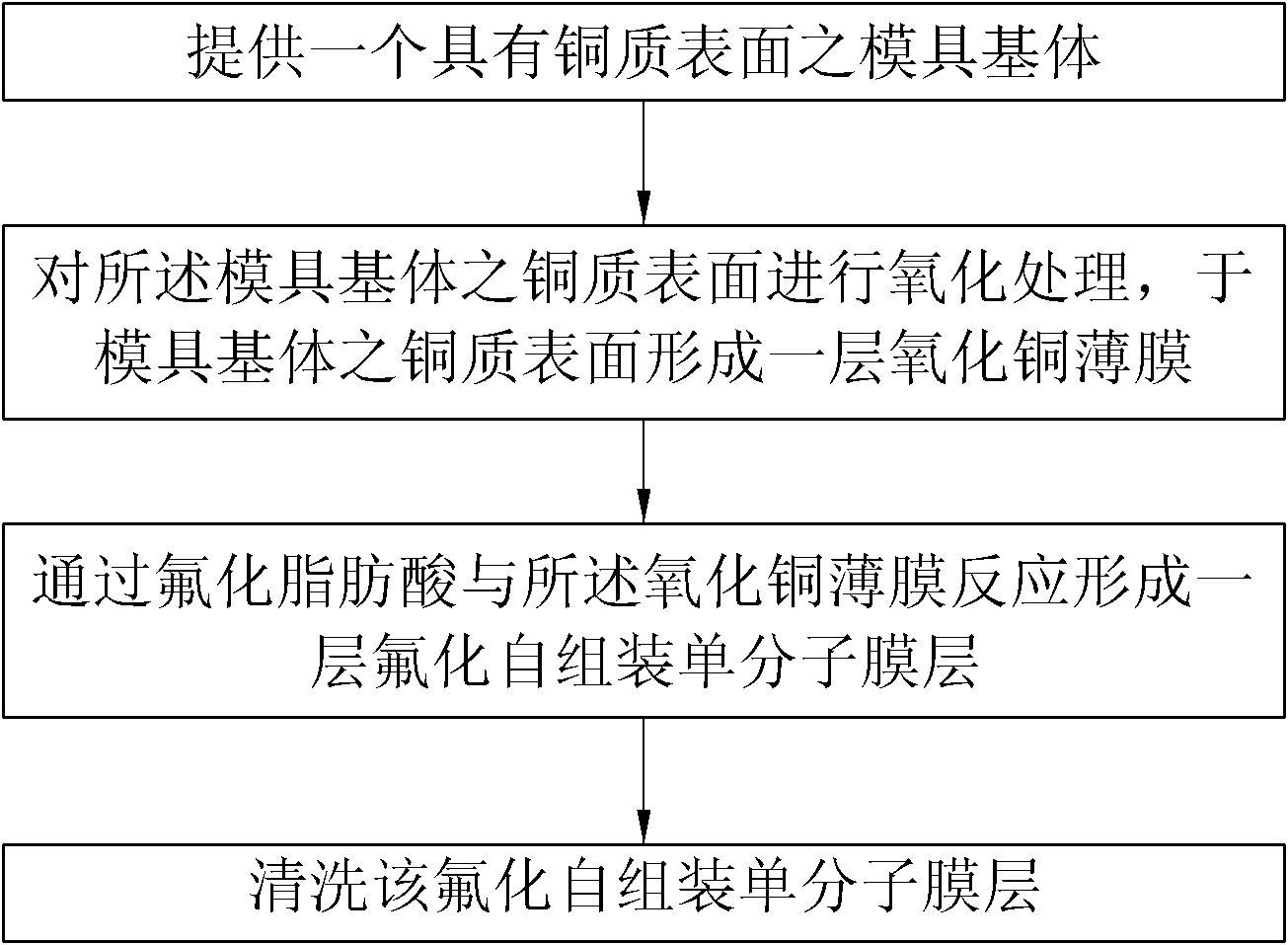
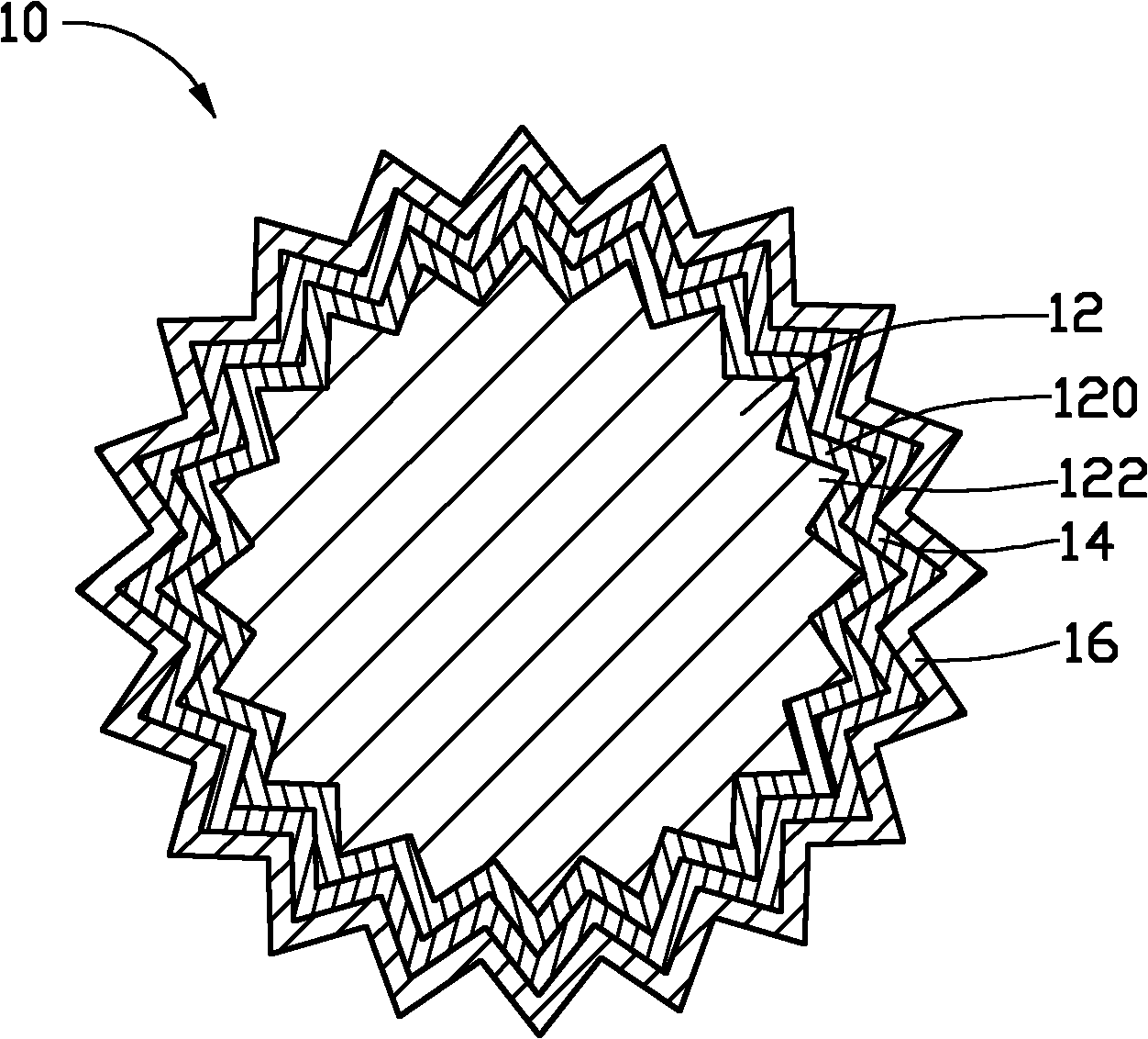
[0019] see figure 1 flow chart and see also figure 2 The first embodiment of the technical solution provides a method for manufacturing an optical film processing mold 10. The method includes the following steps: (1). Provide a mold base 12 with a copper surface 120; (2). The copper surface 120 of the mold base 12 is oxidized to form a layer of copper oxide film 14 on the copper surface 120 of the mold base 12; (3). A layer of copper oxide film 14 is formed by the reaction of fluorinated fatty acid with the copper oxide film 14 Fluorinating the self-assembled monomolecular film layer 16; (4). Cleaning the fluorinated self-assembled monomolecular film layer 16.

[0020] The mold base 12 provided in step (1) with a copper surface 120 can be a copper roller, of course, the mold...


PUM


Abstract

The invention discloses an optical film processing die, which comprises a die substrate, a copper oxide film and a film layer, wherein the die substrate is provided with a copper surface; the copper oxide film is formed on the copper surface; and the film layer is formed on the surface of the copper oxide film, and is a fluorinated self-assembly monomolecular film layer with high hydrophobicity. The die disclosed by the invention has the characteristic of easiness in demolding. The invention further provides a manufacturing method of the optical film processing die.

Description

technical field [0001] The invention relates to the technical field of molds, in particular to a processing mold and a manufacturing method of the processing mold. Background technique [0002] With the development of optoelectronic technology, liquid crystal displays have gradually attracted the attention of consumers and industry players, and the sales volume of the products has also maintained a high growth rate. Among them, the imaging method of the liquid crystal display is driven by the switch of the electric field and displays a high-quality picture, and the liquid crystal panel itself cannot emit light, and the display light source must be provided by the backlight module. [0003] The optical film is one of the components of the backlight module, and its manufacturing technology is also one of the most critical technologies in the manufacture of the backlight module. The main function of the optical film in the backlight module is to use the microstructure on its s...

Claims


Application Information

Patent Timeline
Patent Type & Authority Applications(China)
IPC IPC(8): C23C28/00C23C22/02
Inventor 许嘉麟
Owner HONG FU JIN PRECISION IND (SHENZHEN) CO LTD
Why Eureka
Try Eureka