

PMOS (p-channel metal-oxide-semiconductor field-effect transistor) source/drain region ion implantation method and corresponding device manufacturing method
A device manufacturing method and ion implantation technology, which is applied in semiconductor/solid-state device manufacturing, electrical components, circuits, etc., can solve problems such as the uneven depth of ultra-shallow junctions, and achieve the effect of reducing the difficulty of the process
- Summary
- Abstract
- Description
- Claims
- Application Information
AI Technical Summary
Problems solved by technology
Method used
Image

Examples
Embodiment Construction
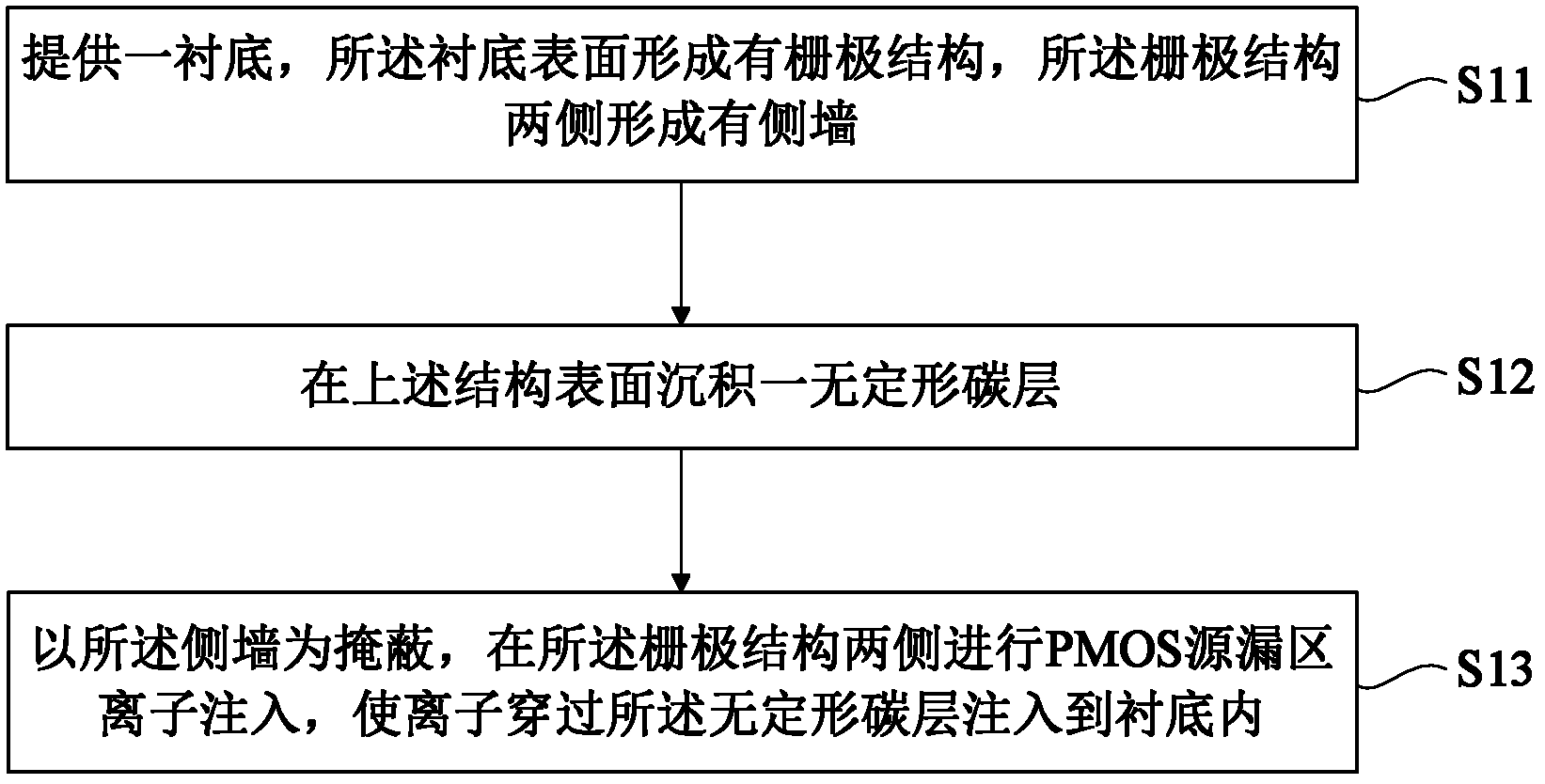
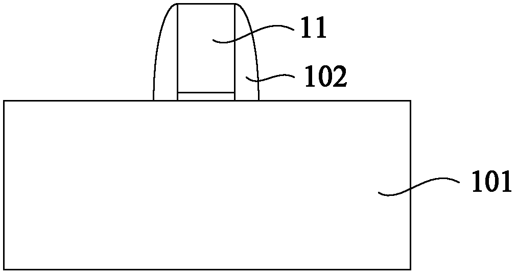
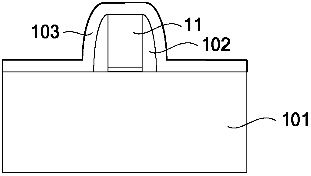
[0038] The specific embodiments of the present invention will be described in detail below in conjunction with the accompanying drawings.
[0039] The core idea of the present invention is to provide a PMOS source-drain region ion implantation method and a corresponding device manufacturing method, using the characteristics that the amorphous carbon layer can be completely removed and will not cause silicon depressions, and the amorphous carbon layer is used as the PMOS source The pad layer of ion implantation in the drain region can reduce the range of implanted impurities in the silicon substrate without basically changing the distribution of implanted impurities, so that ultra-shallow junctions that are shallower than conventional methods can be obtained; or while maintaining ultra-shallow In the case of constant junction depth, the energy of implantation is increased, thereby alleviating the demand for high-dose, low-energy ion implantation in the process to a certain ext...
PUM
 Abstract
Description
Claims
Application Information