Splitting grid memory cell and operation method thereof

A technology of storage unit and operation method, applied in information storage, static memory, read-only memory, etc., can solve the problems of high cost and high cost of photomask, and achieve the effect of simplifying process steps, improving yield, and ensuring reliability

Active Publication Date: 2012-05-02
SHANGHAI HUAHONG GRACE SEMICON MFG CORP
View PDF6 Cites 9 Cited by
  • Summary
  • Abstract
  • Description
  • Claims
  • Application Information

AI Technical Summary

Problems solved by technology

However, due to the high cost of the photomask, the cost of manufacturing the split gate memory cell in the prior art is relatively high

Method used


Image

  • Splitting grid memory cell and operation method thereof
  • Splitting grid memory cell and operation method thereof
  • Splitting grid memory cell and operation method thereof

Examples


Embodiment Construction

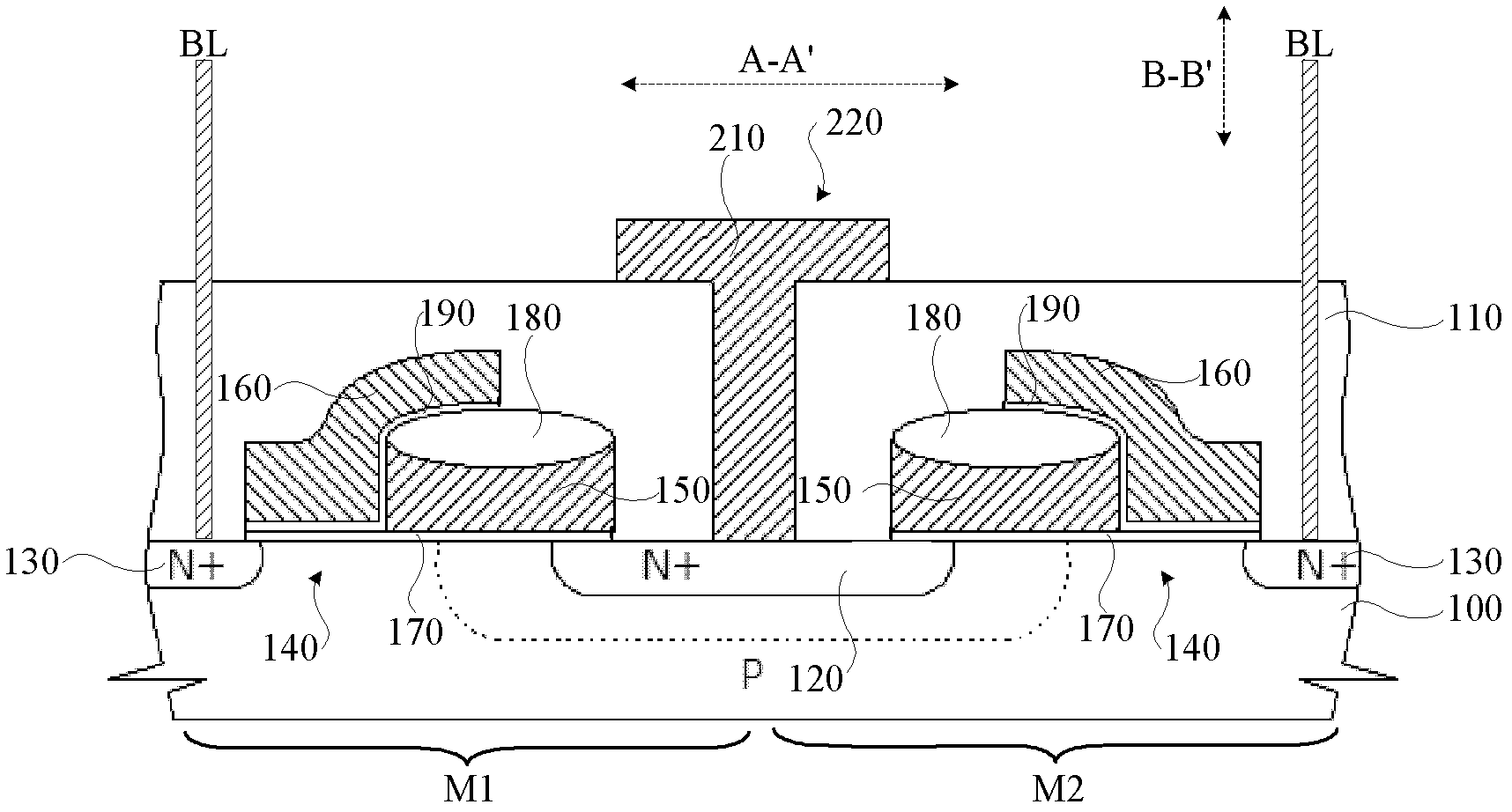
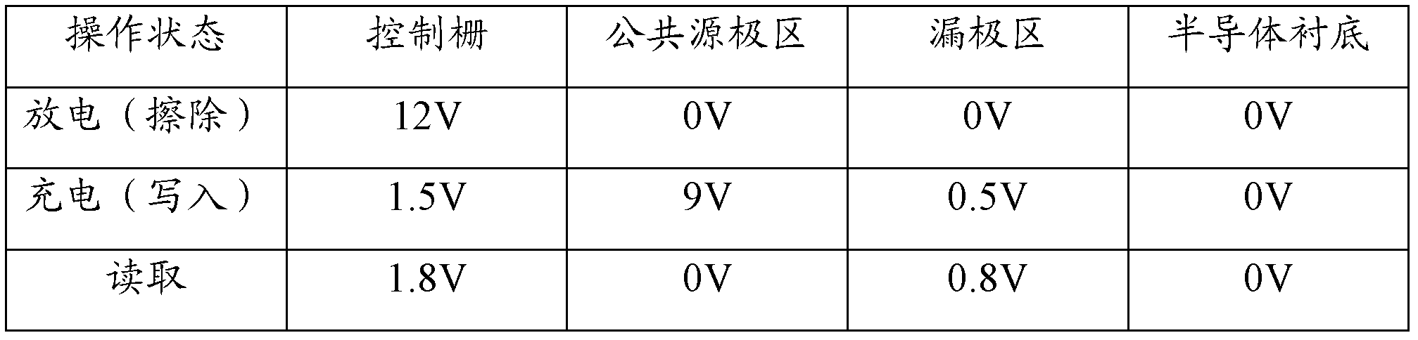
[0038]From the foregoing analysis, it can be seen that in the prior art, the voltage required for erasing the memory cell is 12V, and the positive 12V voltage is applied to the control gate, so it is necessary to form a 12V power supply circuit, but the technology in the art As is known to all, the size of the 12V device is relatively large, the production process is complicated, and the manufacturing cost is relatively high, which results in a large overall size and high cost of the memory unit.

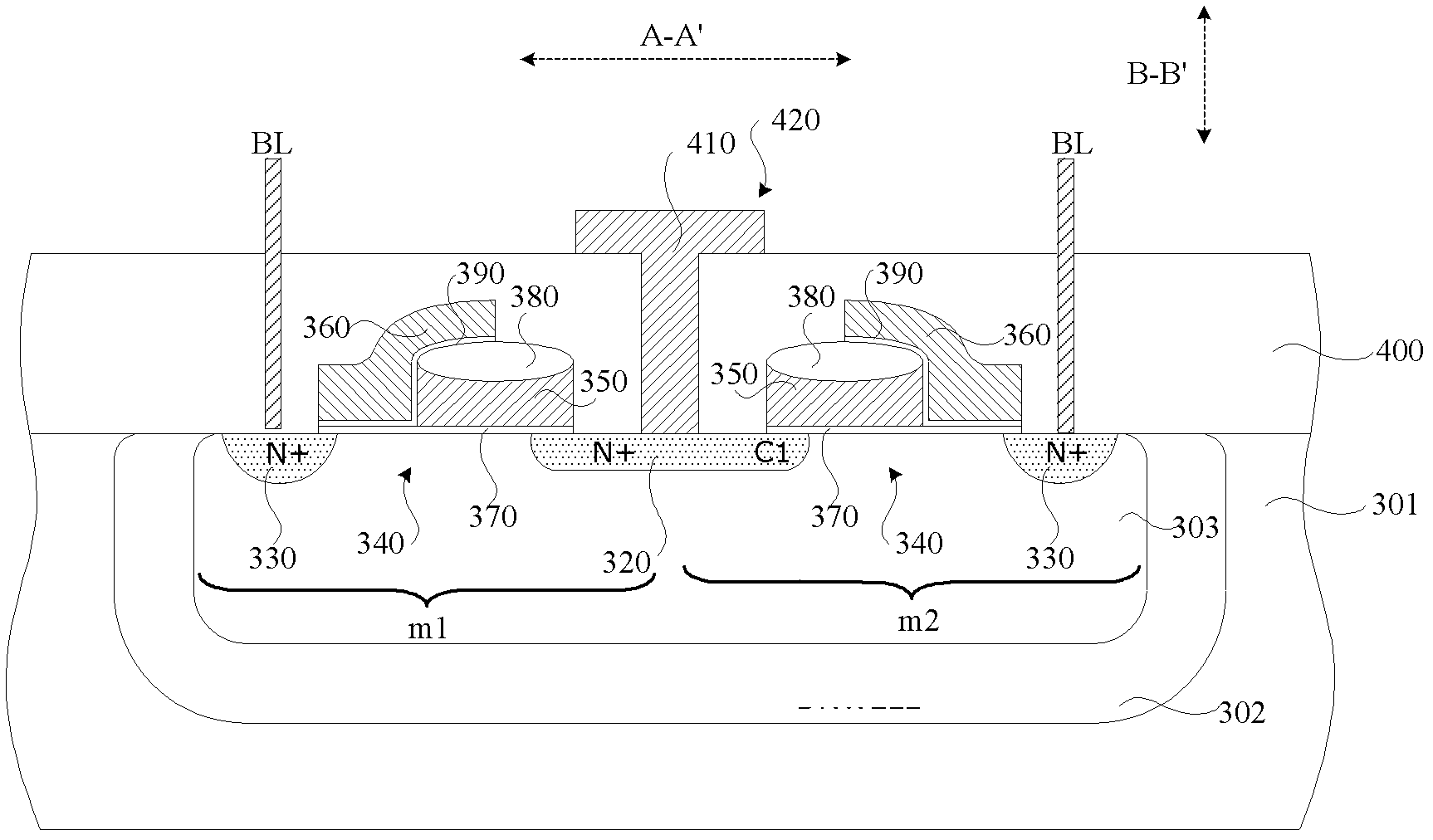
[0039] In order to solve this problem, the split gate memory cell of the present invention forms three doped regions (i.e. the first doped region, the second doped region and the third doped region) sequentially in its semiconductor substrate, so that in When erasing the memory cell, a negative erasing voltage can be applied to the third doped region. In this way, the forward erasing voltage applied to the control gate can be reduced, so that the formation of a 12V power supply circ...


PUM


Abstract

A splitting grid memory cell and an operation method thereof are disclosed. The memory cell comprises: a semiconductor substrate, a floating grid, a control grid and a selection grid, wherein a first doped region, a second doped region and a third doped region are successively formed on the semiconductor substrate; a first diffusion region and a second diffusion region are formed in the third doped region; the floating grid is formed on the semiconductor substrate between the first diffusion region and the second diffusion region; a first side of the floating grid is overlapped with parts of the first diffusion region; the control grid is formed on the semiconductor substrate between a second side of the floating grid and the second diffusion region; an insulating oxide layer is formed between the control grid and the second side of the floating grid; the selection grid is formed on the semiconductor substrate in the first diffusion region; a doped type of the first doped region is the same with the doped type of the third doped region and is opposite to the doped type of the second doped region. By using the memory cell and the method of the invention, a size of the memory cell can be effectively reduced; a quality of the memory cell can be improved and manufacturing costs can be reduced.

Description

technical field [0001] The invention relates to a semiconductor storage device, in particular to a split gate storage unit and an operation method thereof. Background technique [0002] Non-volatile memory refers to a storage device capable of retaining stored data even when power is turned off. Generally, nonvolatile memory devices include erasable and writable read only memory (EPROM), electrically erasable and writable read only memory (EEPROM), and flash EEPROM. There are currently two basic types of non-volatile memory cell structures: stacked gate and split gate structures, in which split gate memory cells are obtained because they can effectively avoid the over-erasing effect and have higher programming efficiency. widely used. [0003] figure 1 A schematic structural diagram of a split gate memory device in the prior art is shown, refer to figure 1 , the memory device includes two memory cells M1 and M2 formed on a P-type semiconductor substrate 100; an N-type fi...

Claims


Application Information

Patent Timeline
Patent Type & Authority Applications(China)
IPC IPC(8): H01L27/115H01L29/423H01L21/8247G11C16/02
Inventor 钱亮杨光军李冰寒
Owner SHANGHAI HUAHONG GRACE SEMICON MFG CORP
Why Eureka
Try Eureka