Liquid crystal panel, method for manufacturing same, and liquid crystal display device
A technology for liquid crystal panels and manufacturing methods, applied in nonlinear optics, instruments, optics, etc., can solve problems such as simple pixel structure, and achieve the effects of wide viewing angle characteristics, high wide viewing angle characteristics, and high contrast characteristics
- Summary
- Abstract
- Description
- Claims
- Application Information
AI Technical Summary
Problems solved by technology
Method used
Image

Examples
Embodiment 1
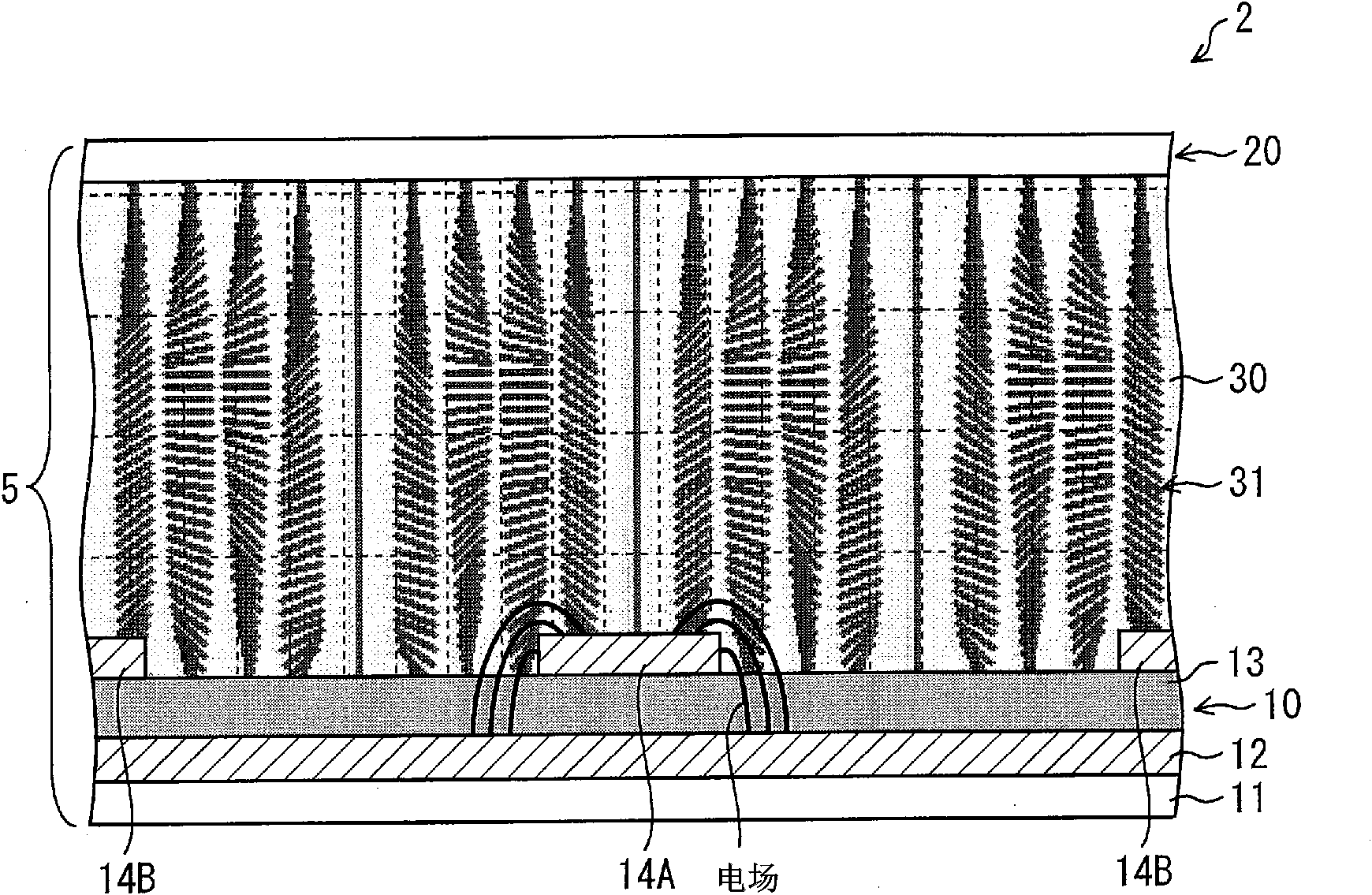
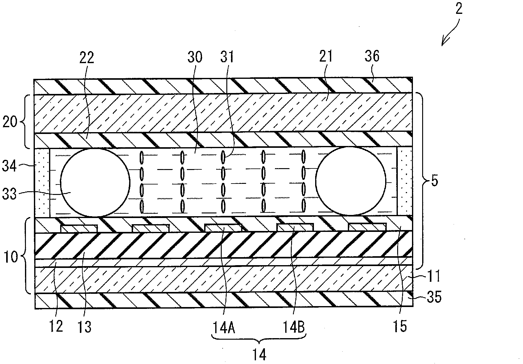
[0130] First, if figure 1 As shown, on the glass substrate 11, by the sputtering method, the entire surface with a thickness of ITO (Indium Tin Oxide: Indium Tin Oxide) film is formed. Thereby, the entire-surface lower-layer electrode 12 covering the entire main surface of the glass substrate 11 is formed.
[0131] Next, silicon nitride (SiN) having a relative permittivity ε=6.9 was deposited by sputtering so as to cover the entire surface of the lower layer electrode 12 . As a result, on the lower layer electrode 12, a layer of thickness d=0.1 μm made of the aforementioned SiN is formed. The insulating layer 13.
[0132] Next, on the upper insulating layer 13, as an upper layer electrode, with a thickness= The electrode width L=2.6 μm, the electrode interval S=8.0 μm, and the comb-shaped electrodes 14A and 14B made of ITO were formed.
[0133] Next, on the above-mentioned insulating film 13, in the manner of covering the above-mentioned comb-shaped electrodes 14A, 14...
Embodiment 2
[0143] Actual measurement T and SimT were obtained in the same manner as in Example 1, except that FFS drive was used instead of comb drive in Example 1.
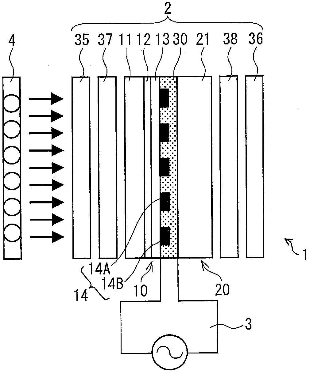
[0144] That is, in this example, the same material and process as in example 1 were used to manufacture the same liquid crystal panel 2 as in example 1, and on the backlight 4, as in example 1, the measured T was measured with "BM5A". In addition, as in Example 1, SimT was obtained by simulation using "LCD-MASTER" when a model having the same FFS structure as in Example 1 was driven by FFS under the same conditions as the above-mentioned actual measurement.
[0145] The above-mentioned SimT, the relative permittivity ε and thickness d of the insulating layer 13, and the electrode width L / electrode spacing S of the comb-tooth-shaped electrodes 14A, 14B are shown in Table 1, and are shown in Table 1 together with the measured T and electric energy EL. Table 8. In addition, in Figure 5 (a) represents the applied voltage in ...
Embodiment 3
[0172] Except that in Example 2, the thickness of the insulating layer 13 was changed from 0.1 μm to 0.3 μm Other than that, SimT was obtained in the same manner as in Example 2.
[0173] The above SimT, the relative permittivity ε and thickness d of the insulating layer 13, and the electrode width L / electrode spacing S of the comb-shaped electrodes 14A and 14B are shown in Table 1, and are shown in Table 8 together with the electric energy EL. . In addition, in Figure 6 (a) represents the applied voltage in the above simulation, and at Figure 6 In (b), it means that through the above simulation, in Figure 6 In (a), the transmittance, the director distribution of the liquid crystal molecules 31 , and the equipotential curve when a voltage of 6 V is applied to the comb-shaped electrodes 14A and 14B, respectively. In addition, in Figure 6 (c) shows the display state of one pixel when the power is turned off and when the power is turned on in the above simulation.
PUM
| Property | Measurement | Unit |
|---|---|---|
| thickness | aaaaa | aaaaa |
| thickness | aaaaa | aaaaa |
| thickness | aaaaa | aaaaa |
Abstract
Description
Claims
Application Information