Light-emitting diode and formation method thereof

A technology of light-emitting diodes and electrodes, which is applied to electrical components, electrical solid-state devices, circuits, etc., can solve the problems of long etching time and low yield, and achieve the effects of saving etching time, high yield, and preventing short circuits.

Inactive Publication Date: 2012-05-09
ZHANJING TECH SHENZHEN +1
View PDF1 Cites 13 Cited by
  • Summary
  • Abstract
  • Description
  • Claims
  • Application Information

AI Technical Summary

Problems solved by technology

However, since the thickness of the epitaxial structure and the buffer layer of the light-emitting diode is relatively thick, generally 4-8 microns, if the buffer layer needs to be completely etched and part of the substrate needs to be etched, a long etching time will be required, resulting in a lower yield. Low

Method used


Image

  • Light-emitting diode and formation method thereof
  • Light-emitting diode and formation method thereof
  • Light-emitting diode and formation method thereof

Examples


Embodiment Construction

[0031] The embodiments of the present invention will be further described in detail below in conjunction with the accompanying drawings.

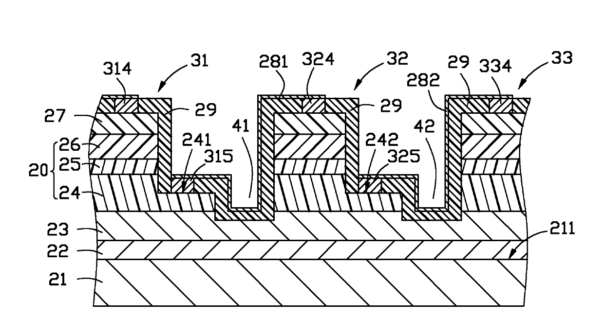
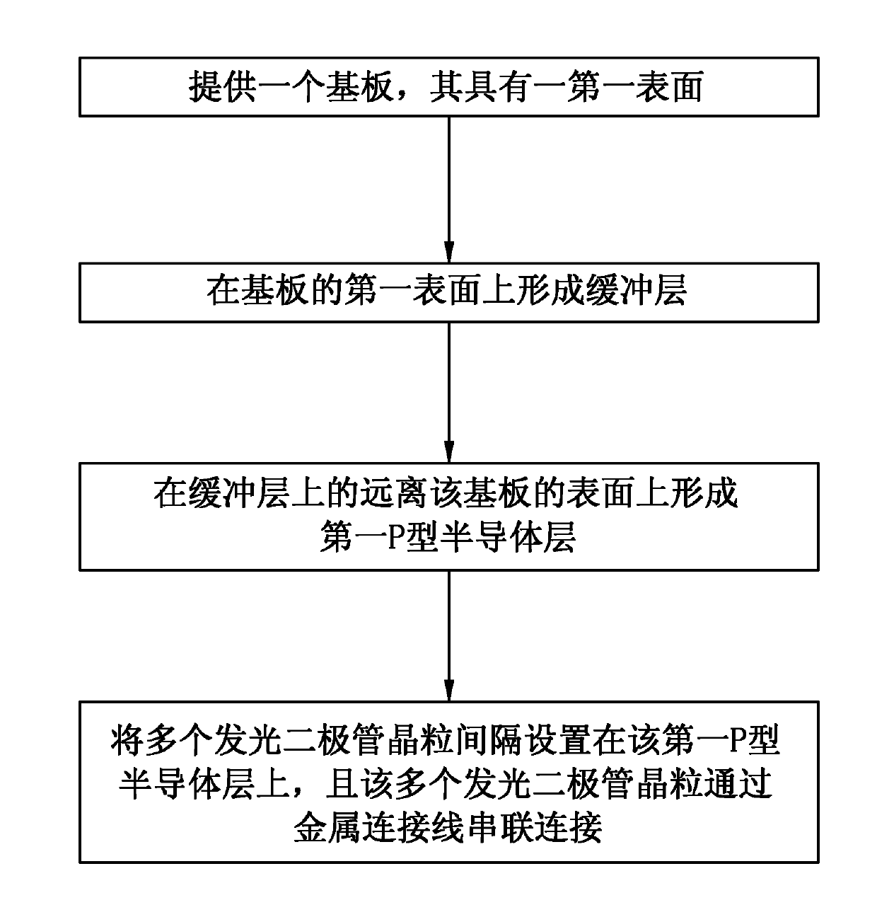
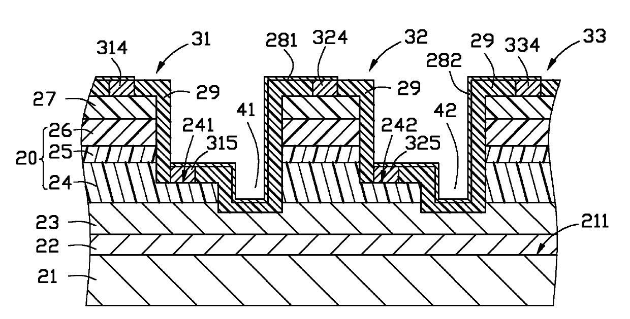
[0032] See figure 1 , An embodiment of the present invention provides a light emitting diode 100, which includes a substrate 21, a buffer layer 22 formed on the substrate 21, a first P-type semiconductor layer 23 formed on the buffer layer 22, and epitaxially grown on the buffer layer 22 on the light-emitting diode epitaxial structure 20. In this embodiment, the light emitting diode epitaxial structure 20 includes an N-type semiconductor layer 24, an active layer 25, and a second P-type semiconductor layer 26.

[0033] The substrate 21 is usually sapphire (Sapphire), silicon carbide (SiC), silicon (Si), gallium arsenide (GaAs), lithium metaaluminate (LiAlO) 2 ), magnesium oxide (MgO), zinc oxide (ZnO), gallium nitride (GaN), aluminum nitride (AlN), or indium nitride (InN) and other single crystal substrates. In this embodiment, the substrate 21...


PUM


Abstract

The invention relates to a light-emitting diode which comprises a baseplate, a buffer layer, a first P-type semiconductor layer and a second P-type semiconductor layer, wherein the baseplate is provided with a first surface, and the buffer layer is formed on the first surface of the baseplate; and the first P-type semiconductor layer is arranged on the surface, far from the baseplate, of the buffer layer; and multiple light-emitting diode grains are arranged on the first P-type semiconductor layer at intervals and are connected in series through metal connecting lines. The invention also relates to a formation method of the light-emitting diode.

Description

Technical field [0001] The present invention relates to a light-emitting diode, in particular to a light-emitting diode with high yield and capable of directly using AC power supply and a method for forming the light-emitting diode. Background technique [0002] Currently, Light Emitting Diode (LED) has been widely used in many fields due to its low power consumption, long life, small size, and high brightness. [0003] Generally, a light emitting diode includes a substrate, a buffer layer formed on the substrate, and a light emitting diode epitaxial structure epitaxially grown on the buffer layer. The light emitting diode epitaxial structure includes an n-type semiconductor layer, an active layer, and a p-type semiconductor layer sequentially formed on the buffer layer. When the light emitting diode uses AC power supply, the light emitting diode epitaxial structure needs to be etched into a plurality of light emitting diode chips connected in series. Specifically, the light-emit...

Claims


Application Information

Patent Timeline
Patent Type & Authority Applications(China)
IPC IPC(8): H01L25/075H01L33/12H01L33/20
CPCH01L33/44H01L33/62H01L27/156H01L2224/24
Inventor 洪梓健沈佳辉
Owner ZHANJING TECH SHENZHEN
Why Eureka
Try Eureka